
Abstract
Porous amorphous silicon carbide (P-aSiC) was prepared by an electrochemical etching method. The surface morphology of the samples was measured by an atomic force microscope (AFM). Photoluminescence (PL) and PL excitation spectra of the samples were measured at room temperature. We observed clear dependence of PL spectra and morphology on fabrication conditions. Based on these results, we propose the emitting mechanism of the PL from the samples.
Export citation and abstract BibTeX RIS

Content from this work may be used under the terms of the Creative Commons Attribution-NonCommercial-ShareAlike 3.0 licence. Any further distribution of this work must maintain attribution to the author(s) and the title of the work, journal citation and DOI.
1. Introduction
Two decades ago, Canham first established visible room temperature PL from porous silicon (PSi) [1]. This work paved the way for solving the optical disadvantages of indirect gap semiconductors. In comparison with Si, Silicon Carbide (SiC) possesses much better electronic properties, such as wide band gap energy, high melting point, high thermal conductivity and large breakdown voltage. These distinctive properties allow the material to work in extremely harsh conditions and environments. Recently, it was found that PSiC exhibited strong visible PL in the blue–green region and it has attracted much research interest due to possible applications of SiC in blue–green light-emitting diodes or photo-detectors [2].
Many papers have reported on the PL spectra of the material, but until now, the origin of the strong visible PL from porous SiC has not been clearly understood [3, 4]. In this research, we present the results of a systematic study on the dependence of the PL spectra and the surface morphology of the porous structures on the fabrication processes. We also propose an emission mechanism for the visible PL of porous aSiC (P-aSiC).
2. Experimental
P-aSiC thin films were obtained by electrochemical etching/anodization from aSiC thin films in hydrofluoric acid (HF) aqueous electrolyte with the aid of H 2 O 2 or Triton surfactants [5]. The etching process was carried out at the Institute of Materials Science (IMS), Vietnam Academy of Science and Technology (VAST). The aSiC thin films were fabricated at the Laboratory of Electronic Components, Materials and Technology, DIMES, Delft University of Technology, the Netherlands, by plasma-enhanced chemical vapor deposition (PECVD) at 400 °C on a standard Si substrate. We used three main types of samples: intrinsic P-aSiC, n-doped P-aSiC and p-doped P-aSiC. The film thickness is 3 μm. All of the samples were anodized by using a voltage constant source. The output voltage (260 V for all samples) was applied to the load consisting of a sample connected in series with a 180 kΩ resistor. All of the anodization processes were carried out in 30 min.
3. Results and discussion
To examine the morphology of the porous layer, the atomic force microscope (AFM) measurements were performed. The AFM images show that the pore diameter varies from several tens of nm to several hundreds of nm, and the pore depth is in the range of several tens of nm. With decreasing HF concentration, the diameter and depth of the pores increased with lower pore density, as shown in figure 1.

Figure 1 AFM images of intrinsic P-aSiC samples etched with different HF%.
PL measurements were performed at room temperature using a 325 nm line of a He–Cd laser. Figure 2 shows PL spectra of intrinsic P-aSiC samples etched with different HF concentrations. The samples showed very broad PL spectra in the visible and near-infrared region. One may notice that the spectrum has a multiple fringe. We suggest that this phenomenon came from the interference effect. In particular, the SiC thin films worked as a cavity, which caused the multiple reflections inside and thus led to this kind of interference spectrum.

Figure 2 HF concentration dependence PL spectra of intrinsic P-aSiC.
Figure 2 indicates that the PL spectrum depends strongly on the concentration of HF. The PL spectra can be divided into two bands: one band with a PL peak in the near-infrared region at 1.7 eV, the other band with a PL peak in the visible region at 2.3 eV. In addition, the samples etched with a HF percentage of less than 5% have the PL peak at 1.7 eV, and the samples etched with a HF percentage of more than 10% have the PL peak at 2.3 eV. Furthermore, the PL intensity of the 1.7 eV band and 2.3 eV band showed totally opposite behaviors when changing the HF concentration. For the PL band at 1.7 eV, when increasing the concentration of HF, the PL intensity increased. In contrast, for the PL band at 2.3 eV, when increasing the concentration of HF, the PL intensity decreased.
All of the PL spectra were fitted with two Gaussian functions (figure 3). This showed that the spectra are composed of two bands with peak energies at 1.7 and 2.3 eV, which are denoted as curve 1 and curve 2, respectively. These photon energies are unchanged between the different samples, which indicates that PL emerged from two luminescent sources. In addition, the PL band of the unetched samples, shown in figure 4, completely coincided with Curve 1 of the etched sample. As a result, this indicates that they originated from the same states. Figure 5 demonstrates clearly the tendencies of the PL intensities of curve 1 and the curve 2 with the change in HF concentrations. Therefore, we can confirm that the PL spectra of intrinsic P-aSiC are composed of the two PL bands at 1.7 and 2.3 eV, and these two curves exist simultaneously. In addition, the origins of these two PL curves are completely different.

Figure 3 Fitting results of PL spectra of intrinsic P-aSiC with 5% and 15% HF. Both were fitted with two Gaussian functions with peak energies at 1.7 and 2.3 eV.

Figure 4 PL spectrum of bulk aSiC.

Figure 5 Integrated PL intensity of curve 1 and curve 2 in figure 2 as a function of HF concentration.
Figure 6 shows the PL spectra of n-type and p-type P-aSiC. Unlike the intrinsic samples, we could observe the PL only in the visible region. Furthermore, the PL peak photon energy shifted to a higher energy at 2.7 eV for both n-type and p-type samples. However, the PL intensity of the doped P-aSiC showed exactly the same tendency as the visible band of the intrinsic samples. The higher PL intensity was observed for the lower HF concentration. This indicates that the nature of the luminescence of the doped samples is somewhat similar to the visible bands of the intrinsic samples.

Figure 6 HF concentration dependence PL spectra of n-type P-aSiC (a) and p-type P-aSiC (b).
For a better understanding of the electronic structures and PL mechanism of P-aSiC, PL excitation (PLE) measurement was performed. A Xenon lamp connected to a monochromator was used as the excitation light source. The PL spectra were detected using a 30 cm monochromator. The excitation wavelength dependences of the PL spectra of the intrinsic sample are plotted in figure 7(a). When changing the excitation energy, the PL peak photon energies remained almost constant. Otherwise, the PL intensity changed drastically. figure 7(b) shows the normalized PLE spectra with many selected emission photon energies. We observed two absorption peaks: one at 3.2 eV (∼390 nm) and the other at about 2.8 eV (∼443 nm). Furthermore, at higher emission energies, the absorption peak at 2.8 eV is more pronounced, and at lower emission energies, the absorption peak at 3.2 eV is more pronounced. The results confirmed that there are two luminescent centers that exist simultaneously.

Figure 7 PL and PLE spectra of 1% HF intrinsic P-aSiC.
Up to now, the origin of the PL of P-aSiC has remained unclear. Regarding the origin of the visible PL from PSi, the quantum confinement effect was believed to be the main reason. However, no explicit evidence of quantum confinement was observed in our samples for two reasons. Firstly, the pore diameters were too large in comparison with the SiC exciton Bohr radius (∼49 Å). Secondly, we found no PL peak shift when changing the excitation energy. Therefore, the emission mechanism of PSiC is predicted to be very different from that of PSi. In this report, we propose an emission mechanism of P-aSiC related to surface states and surface regions. In order to understand how the etching process could help to generate strong visible PL spectra from a weak luminescence material, we paid attention to the fabrication process in more detail. The chemical reactions throughout the electrochemical etching process are believed to be as follows [6]:
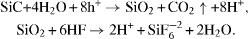
From these reactions, we may infer that first, a SiO 2 layer was formed on the surface of the material. This layer then interacted with HF to form the porous structure alongside producing H + ions on the surface of the sample. Several percent of HF are needed to dissolve the entire amount of SiO 2. Now, referring to the PL results, figure 5 indicates that when increasing the concentration of HF, the intensity of the visible PL band decreases. This behavior is consistent with the fact that the amount of SiO 2 also decreased when we added more HF. So we come to the first suggestion that SiO 2 must play an important role in the visible PL of P-aSiC.
However, if SiO 2 is the only factor that affects the visible PL of P-aSiC, the situation becomes the same as in the case of PSi, where the observed PL peak photon energies were always less than 2 eV [7, 8]. As a result, we might not be able to explain the reason for the blue–green PL from P-aSiC. Therefore, we took into account the contribution of carbon (C). The report of Seo et al on carbon-doped silicon-rich silicon oxide (SRSO) [9] indicated that C is essential for the blue–green luminescence of SRSO films. To verify this hypothesis, the energy-dispersive x-ray spectroscopy (EDS) measurement was taken with the doped samples in order to examine the chemical compositions of the surface layer of P-aSiC thin films. This measurement was done in the IMS-VAST. Table 1 shows the EDS results of n-type samples and displays the atomic percentage of elements C, Si and O. When the concentration of HF increased, the content of the O element decreased gradually, while the content of C and Si remained almost constant. In addition, the bulk sample possessed almost no O. This is conclusive evidence that proves our assumption about the behavior of SiO 2 when changing the content of HF. In other words, this result agrees well with our suggestion that defects in SiO 2 with the contribution of C originated the visible PL of P-aSiC.
Table 1. EDS results of n-type P-aSiC
| 0.02% HF | 23.857 | 21.872 | 51.960 |
| 0.05% HF | 31.698 | 15.710 | 50.610 |
| 0.1% HF | 26.760 | 13.856 | 57.180 |
| 0.3% HF | 31.978 | 4.718 | 61.458 |
| 0.5% HF | 37.847 | 2.833 | 57.233 |
| Bulk (un-etched) | 37.642 | 0.285 | 59.102 |
Regarding the origin of the near-infrared PL, we suggest that the PL band in the near-infrared region originated from H-related compounds in the surface states of intrinsic P-aSiC. Figure 5 indicates that the PL intensity of the near-infrared band becomes stronger when the concentration of HF increases, so there must be a relationship between the near-infrared PL and the H-related bonds. However, the exact nature of this PL band requires further investigation.
4. Conclusion
P-aSiC samples have shown the visible PL spectra at room temperature. The PL spectra were found to contain two components, which correlates with the concentration of surface chemical elements in P-aSiC. From the obtained results, we confirmed that the quantum confinement effect was not the origin of the visible emission from the samples. The actual origin was attributed to surface-related states. We suggested that the PL band at 2.3 or 2.8 eV originates from Si–O related bonds with the aid of C, and the PL band at 1.7 eV originates from Si–H related bonds. For future research, we plan to measure the Raman scattering and the time-resolved PL measurements to verify our hypothesis and to clearly understand the relaxation mechanism of PSiC. We also plan to continue the research on the impact of doping on the PL properties of P-aSiC.
Acknowledgment
This work was supported by the Multidisciplinary Research Laboratory System (MRL), the Graduate School of Engineering Science, Osaka University.