

Abstract
Nanocavities and cavities are known to be efficient gettering sites for metallic impurities in silicon. Here, we report results from implanted 〈100〉 silicon at room temperature with 50 keV helium ions at a dose of 3×1016 cm−2. Due to its low solubility, He segregates in gas-vacancy complexes and forms nanobubbles. Then, during an N2 ambient annealing at 800 °C using either rapid thermal annealing (RTA) or conventional furnace annealing, nanobubbles grow and He is released from the nanobubbles by gas exodiffusion, leading to (nano)cavities' formation. (Nano)cavities and residual defects were observed by transmission electron microscopy (TEM). The fraction of retained helium was shown to decrease with annealing time according to the first-order gas release model. Two nucleation-growth mechanisms involved in the growth of these (nano)cavities have been studied. A remarkable result shows evidence about the balance-time dependence of the two mechanisms involved in the growth process of (nano)cavities. At the very beginning (30 s) of the annealing, the main mechanism is the migration-coalescence including nanobubbles and vacancy-helium complexes leading to the cavities' formation. Then, the Ostwald ripening mechanism, related to the helium exodiffusion, between the nanocavities and cavities appeared.
Export citation and abstract BibTeX RIS

Content from this work may be used under the terms of the Creative Commons Attribution-NonCommercial-ShareAlike 3.0 licence. Any further distribution of this work must maintain attribution to the author(s) and the title of the work, journal citation and DOI.
1. Introduction
(Nano)cavities induced by hydrogen or helium implantation are known to be very efficient traps for unwanted metallic impurities in silicon [1–8]. The widely accepted mechanism of trapping (or gettering) is the chemisorption at the internal surface of the (nano)cavities [4]. The gettering procedure is a method of removing impurities from the active device region. Hence it has the most potential to satisfy the requirements on the predicted device layer [9]. Griffioen et al [10] were the first to show that helium, when implanted into silicon may form small bubbles and then outdiffuse during annealing, leaving empty cavities. However, the helium desorption kinetics generally observed at the temperature used to form cavities (higher than 700 °C) is not completely understood. In this paper, we show the results of the evolution of (nano)cavities formed at 800 °C as a function of the annealing time. The latter allows us to understand the role of the helium desorption in the formation of (nano)cavities.
2. Experimental
Czochralski (CZ), 〈100〉 oriented, n-type silicon wafers, 500 μm thick, were used in this study. They were implanted at room temperature with 50 keV helium ions by means of a Bernas-Nier source-type implanter at a dose of 3×10¹⁶ He m −2. According to the simulation program, named the stopping and range of ions in matter (SRIM08 or TRIM08) [11], the mean projected range (R P ) of these ions is ∼450 nm.
The implantation of helium ions into the samples was followed by the heat treatment in N 2 atmosphere, using either a rapid thermal annealing (RTA) system or a conventional furnace annealing (CFA). The annealing times range was from 30 s to 4 min for RTA and 60 min for CFA at 800 °C. This temperature is expected to form a cavity layer. The morphology of the cavity layer was observed by transmission electron microscopy (TEM) using a FEI Tecnai G 2 F20 microscope. To avoid any electron irradiation we performed TEM observations at 150 kV. The thinned samples in cross section were prepared by mechanical thinning. TEM analyses were performed along the 〈110〉 direction, for cross view analyses.
3. Results and discussion
Helium implants in silicon, at a concentration equal to or higher than the critical value of 3×1020 cm −3 [12], induce nanobubble formation. Nanobubbles can be observed directly by TEM analyses (e.g. figure 1). Figure 2 shows a TEM micrograph of an as-implanted sample with 50 keV He ions at a fluence of 3×10¹⁶ He cm −2. Also reported in this figure are the depth profiles of vacancies and He as obtained by SRIM08 calculations.
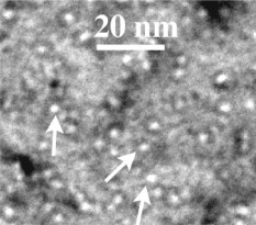
Figure 1 TEM image of nanobubbles in the as-implanted silicon sample with helium at 3×1016 cm −2 and 50 keV.
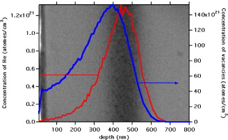
Figure 2 TEM cross section of an as-implanted sample with 50 keV and 3×1016 cm −2 He ions. The depth profiles of He and vacancy distribution as obtained by a SRIM08 calculation is reported for comparison.
Nanobubbles of 2–3 nm in diameter are present from sample surface to 700 nm, corresponding to the end of the depth profile of He and vacancy distribution (figures 2–4). The peak of nanobubble concentration is localized at the depth shallower than the one of the He projected range, in a region where the radiation damage peak is located according to SRIM08 calculations.
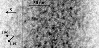
Figure 3 TEM image of helium-implanted silicon at 50 keV and 3×1016 cm −2, without anneal. The middle part limited by two vertical lines is the center of nanobubble layer. The S letter indicates the sample free surface.

Figure 4 Density of nanobubbles 2–3 nm just after implantation. The concentration profiles of He and vacancies obtained by TRIM 2008, for the helium implantation at 50 keV and 3×10¹⁶ He cm −2, are also reported in the same figure. The L C letter in the figure indicates the center of nanobubble region that contains the highest concentration.
TEM observations have been performed as well on wafers annealed for various times at 800 °C. Figure 5 is a TEM micrograph of a 50 keV—3×10¹⁶ He cm −2 implanted sample annealed for 30 s at 800 °C.

Figure 5 Cross-sectional TEM micrograph of Si implanted with 3×10¹⁶ He cm −2 at 50 keV and RTA annealed for 30 s at 800 °C.
We will show below that the main part of He has been removed from the sample after annealing. So, for clarity, we design as (nano)cavities the nanostructures observed after nanobubble evolution during annealing.
It can be seen that, even for this short annealing time, the large cavities (with diameter up to 10 nm) at the region II in figure 5 are formed. However, numerous small nanocavities (2–3 nm) are also present in two areas. The first, marked region I in the figure, is located between the surface and the large cavity layer (region II). The latter corresponds to the located region of the radiation damage peak. The second area where the nanobubbles are present is located in the region marked III, just behind the large cavity layer. The nanocavities are distributed until the end of the He profiles (∼700 nm). Besides cavities, other defects can be identified by using weak beam conditions of TEM analyses: {311} interstitial defects (figure 6). These defects are well-known in silicon (see for examples [13–15]). We have schematized in figure 7 the regions I–III with the structures, respectively, present after annealing.
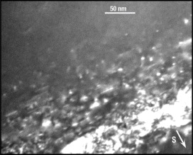
Figure 6 XTEM observation of {311} rod-like defects (located behind the buried layer) by means of weak beam 2 g condition obtained in Si implanted with 3×10¹⁶ He cm −2 at 50 keV and after a 30 s RTA annealing (800 °C).

Figure 7 Schematic view of the repartition, in regions I–III, of (nano)cavities and defects induced by 50 keV He implantation following by annealing at 800 °C.
For longer annealing times (up to 4 min for RTA), we observe the same features as reported in the case of 30 s, i.e. nanocavities in two sides of cavity band and {311} defects behind (see figure 8).
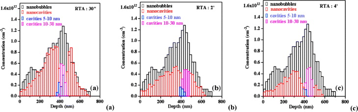
Figure 8 Implanted samples (E=50 keV, D=3×10¹⁶ He cm −2). Comparison of the nanobubble distribution before annealing with the series of observed (nano)cavities after a rapid annealing of (a) 30 s, (b) 2 min, (c) 4 min.
Figure 8 allows us to compare the distributions of all types of (nano)cavities obtained at each annealing time after annealing with the nanobubbles' distribution before annealing. It shows that:
- At 30 s, the distribution profile of the concentration of nanocavities follows the one of nanobubbles, except near the surface (where the nanocavity concentration decreases significantly) and in the region of the large cavities where they disappear completely. We then note the effect of diffusion of the nanocavities towards the surface as well as migration-coalescence processes at the maximum of nanobubble concentration.
- After annealing time ⩾2 min: compared to the nanobubbles we note a significant decrease of the nanocavity concentration at both sides of the cavity band. This confirms the predominance of a diffusion mechanism of vacancies in the second stage.
- Considering the experimental uncertainties, we observe an almost constant concentration of all the cavities between 5 and 30 nm during annealing of 30 s to 4 min. This point is verified by the evaluation of free volumes involved in the band of cavities.
- After 4 min of annealing and even after a furnace annealing during 1 h (figure 9), in front of the band of cavities, the decrease of the distribution is even stronger as we approach either the free surface, or the band of cavities. This leads to the distribution with a peak of 300 nm. This effect may be attributed to the variation of helium exodiffusion rate during annealing.
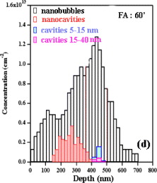
Figure 9 Implanted samples (E=50 keV, D=3×10¹⁶ He cm −2). Comparison of the nanobubble distribution before annealing with conventional annealing for 1 h.
We estimated the theoretical variation of He from the equation used by Griffioen et al [10] for the helium desorption of the first order:

where N He is the number of He atoms in the bubble, being a function of annealing time, d N He /d t is also known as the evolution of the residual fractions of He as a function of annealing time, P is the permeation rate of He in Si, R is the distance from the surface, r b is a bubble radius, E p is the activation energy of permeability, T is annealing temperature and k is Boltzmann constant (∼8.6×10⁻⁵ eV K −1). Integrating this equation gives a rate of helium remaining in a cavity:

with
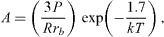
where R=450 nm, r b =2–20 nm and T=800 °C.
From the expression (
For the energy of 50 keV, these calculations show that there are still 97–80% of helium atoms in large cavities for an annealing time varying from 30 s to 4 min. For the nanocavities, the amount of remaining helium decreases with depth. It is practically zero at depth lower than or equal to 100 nm from an annealing time of 4 min.
For an annealing time of 1 h, there is almost no more helium in the nanocavities, whatever their position.
The kinetic evolution of 'nanocavities', through the evolution of vacancies during annealing at 800 °C for energy of 50 keV is summarized in table 1 below.
Table 1. Concentration of vacancies estimated in the cavities and 'nanocavities' after annealing at 800 °C as a function of the annealing time for implantation at 50 keV. All observed (nano)cavity regions have the same thickness.
| 30 | 6.8 | 3.4 | 3.1 | 21 |
| 120 | 7.7 | 5.4 | 2.1 | 8.8 |
| 240 | 1.2 | 5.7 | 1.5 | 8.5 |
We have shown in table 1:
- For the annealing time from 30 s to 4 min, the volume growth of cavities in the band leads logically to an increase in the concentration of vacancies in this band.
- Similarly, for annealing time from 30 s to 4 min, the concentration of nanocavities in the area in front (zone I) and back (zone III) of cavity band (zone II) decreases progressively and also leads to a decrease of the number of vacancies in zones I and III. Then it parallelly leads to a decrease of the loss of helium in the nanocavities in zones I and III. This confirms that the loss of helium favors the diffusion of vacancies out of nanocavities.
- However, the decrease of the vacancy concentration of nanocavities in zone I (in the order of 1014 vacancies cm −2) added to that in zone III (in the order about 1014–013 vacancies cm −2) is two orders of magnitude smaller than the increase of the vacancy concentration in the cavities (in the order of 1–2×10¹⁶ vacancies cm −2). The very probable diffusion of the vacancies (zone II) from the nanocavities (part of zone I near the cavity band and zone III) to the cavities (Ostwald ripening mechanism) cannot, anyway, explain the increase of the vacancy concentration of cavities. The most likely hypothesis is the contribution of vacancies with the distance from 'nanocavities' ⩽1.5 nm and vacancy-He complexes remained stable in the first stage of annealing. This hypothesis is in agreement with the result obtained for the nanobubble concentration compared to the results obtained by other authors in high resolution.
- In the case of annealing of 1 h, we observe a strong decrease in the vacancy concentration of the nanocavities in zone I and particularly we observe the presence of a hollow between the nanocavity and cavity region (see in figure 9). It is therefore likely that after annealing of 4 min, an Ostwald ripening mechanism becomes significant and increases with time.
4. Conclusion
This study has allowed us to show that:
The evolution during the annealing of nanobubble system created by helium implantation is separated into two stages: (i) at the beginning of annealing (⩽30 s), in the center of the nanobubble band with the high density, there is formation of a cavity band by migration coalescence. (ii) Secondly, for higher annealing times, the study on (nano)cavities as a function of the annealing time (in particular with RTA) showed that the concentration of cavities is practically constant. The growth mechanism by diffusion of the vacancies predominates.
At the first stage, the nanobubbles which do not participate in the formation of cavities are found to be almost unchangeable (size, density and distribution in depth). This confirms that only the migration coalescence process occurs at this stage.
At the second stage, all our observations and calculations have shown that the evolution of 'nanocavity' and cavity system were most likely controlled by a diffusion process of 'nanocavities' to the free surface and to cavities (Ostwald ripening mechanism).
The relationship between the rates of helium desorption and the disappearance of the nanocavities has been clearly demonstrated. The phenomenon of vacancy diffusion outside of nanocavities is accelerated by helium exodiffusion. In other words, the activation energy of the vacancies in the nanocavities is lower when the helium exodiffuses [10].
The desorption of helium, especially fast when the system of (nano)cavities is near the free surface, is accompanied by a disappearance of 'nanocavities' located near the free surface.