

Abstract
The emission mechanism in ZnS-capped 3-nm CuInS2 nanocrystals was studied by using time-resolved photoluminescence (TRPL). A typical TRPL spectrum demonstrates two broad emission bands. The spectral shifts as functions of the excitation power density and delay times from the excitation moment prove that both emission bands originate from donor-acceptor pair recombinations. Moreover, the temperature-dependent TRPL measurement revealed the importance of trapping sites in the emission mechanism of CuInS2 nanocrystals.
Export citation and abstract BibTeX RIS

Content from this work may be used under the terms of the Creative Commons Attribution-NonCommercial-ShareAlike 3.0 licence. Any further distribution of this work must maintain attribution to the author(s) and the title of the work, journal citation and DOI.
1. Introduction
Cd-based quantum dots (QDs) or nanocrystals (NCs), such as CdSe and CdTe, and their core/shell systems have been successfully synthesized by different methods [1–5]. High-quality CdSe and CdTe QDs are characterized by their narrow photoluminescence (PL) spectra (full-width at half-maximum of 20–40 nm) resulting from a narrow size distribution, and a high PL quantum yield (QY). These characteristics make them potentially applicable in biological labeling [1–3] and optoelectronic devices, including light emitting diodes and solar cells [4, 5]. Besides many advantageous features, however, the existence of Cd in the mentioned QDs is problematic because of its toxicity and the accumulation of heavy metals in the human body. Recently, in searching for alternatives, some different materials, such as ZnSe, InP, CuInS 2, etc, have attracted much attention [6, 7]. Among them, CuInS 2 (hereafter called CIS), a chalcopyrite semiconductor, seems to be a good candidate from the optical point of view, along with the requirement of Cd-free materials [8–12]. Chalcopyrite semiconductors, such as Cu(In/Ga)(S/Se)2, have been investigated mostly due to their potential in photovoltaic devices, especially for use in space stations, because they are very resistant to cosmic rays. In addition, the quantum structure of chalcopyrite semiconductors enables them to emit in the visible spectral range. Recently, there have been some publications on the synthesis of CIS NCs and their luminescence properties [13–18].
For single crystals of CIS, detailed studies of the optical transitions and the identification of the origin of emission have been reported [9, 11]. For CIS NCs, however, different interpretations of the observed emission properties can be found in literature. Castro et al assigned the observed PL bands in CIS NCs to intrinsic defects based on a comparison between the obtained emission energy and the energy levels from CIS single crystals [13]. In another point of view, Hamanaka et al considered that the emission in CIS NCs originates from radiative recombination after stepwise hopping of electrons and/or holes among surface sites [16].
The aim of this paper is to interpret the optical processes in CIS/ZnS core/shell NCs based on the experimental results obtained from absorption, steady-state PL (SSPL) and temperature-dependent time-resolved PL (TRPL) measurements. The latter technique helped us to make important progress in the determination of the emission origin in CIS NCs. Moreover, temperature-dependent TRPL measurement has helped us to reveal the importance of trapping sites in their emission mechanism.
2. Experimental
For absorption and SSPL measurements, CIS/ZnS NCs were measured in colloidal solution in chloroform. For temperature-dependent TRPL measurements, the samples were prepared as solid close-packed films by dropping CIS/ZnS NCs in chloroform onto a Cu plate that then could bind easily to the cold finger of a closed-cycle helium cryostat. Details of the CIS/ZnS NCs preparation were described in our previous article [18]. For comparison, a pulsed nitrogen laser (emitting at 337.1 nm, ∼1 ns pulse duration and repetition rate of 25 Hz) was used as the excitation source for both SSPL and TRPL measurements. For SSPL, the PL signals were dispersed by a 0.55-m grating monochromator (Horiba Jobin-Yvon iHR550) and then detected by a thermoelectrically cooled Si-CCD camera (Synapse). For the TRPL measurements, the PL signal was dispersed by a 0.6-m double grating monochromator (Jobin-Yvon HRD1) and detected by a fast and sensitive photomultiplier (PMT, H7313 Hamamatsu). The excitation power density was set in the range of 6 kW cm −2 to 1 MW cm −2 on the sample surface by using different combinations of neutral density filters. At each specific wavelength of the spectrum under measurement, an electrical signal pulse from the PMT was recorded showing the corresponding PL-decay curve. Thus, we could determine the PL decay-time at every wavelength in the PL spectrum. Then, by extracting the PL intensity as a function of time delayed from the excitation moment, the whole TRPL spectra at a certain delay time could be reproduced. With a multi-pulse average at each spectral point using a 1.5 GHz digital oscilloscope (LeCroy 9362), the signal-to-noise ratio was significantly improved.
3. Results and discussion
A typical absorption spectrum of the CIS/ZnS NCs dissolved in chloroform is shown in figure 1. The observed shoulder at ∼2.3 eV in the absorption spectrum could be assigned to the excitonic transition in the CIS NCs. The peak energy is about 0.7 eV larger than the bandgap energy (1.53 eV) of CIS bulk crystal, indicating the quantum confinement effect in the studied CIS NCs. The SSPL spectrum measured under the 337.1-nm pulsed laser excitation is also presented (figure 1(b)). A broad PL band with full width at haft maximum of 380 meV and a large Stokes shift of several hundreds of meV are observed. These features suggest that the observed PL band does not originate from the excitonic transition but from recombination of electrons and holes in defect states. To further elucidate the origin of the PL band, TRPL measurement was performed with the close-packed CIS/ZnS NCs. The evolution of the emission with time elapsed from the excitation moment demonstrates two spectral components. At a very long delay time of 1 μs (figure 1(c)), the TRPL spectrum looks similar to the SSPL spectrum of the close-packed CIS/ZnS NCs because at that delay time one can record only the long-lifetime spectral component in the low energy region. A small red-shift of its emission peak energy as compared to that of colloidal CIS/ZnS NCs dissolved in chloroform is expected due to superposition of the two spectral components in the SSPL spectrum, while in the TRPL spectrum only the long-lifetime spectral component in the low energy region is observed. This is also due to energy transfer and/or charge carrier transfer between the close-packed CIS/ZnS NCs, consistent with what was observed in the case of InP/ZnS NCs [19].
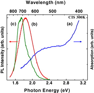
Figure 1 (a) Absorption and (b) SSPL from the 3-nm colloidal CIS NCs dissolved in chloroform; and (c) TRPL spectrum at long delay time (of 1 μs) elapsed from the excitation moment. Note that the TRPL spectrum was taken from close-packed CIS NCs in a thin film.
Deconvolution of the TRPL spectra at some different delay times has been achieved, showing the peak energies of the two spectral components as a function of the delay time (figure 2). The spectral component located at higher energy (∼1.9 eV) decays faster, with a decay-time estimated to be tens of nanoseconds; the other one located at lower energy (∼1.73 eV) decays in several hundreds of nanoseconds. The decay times of both spectral components are very long as compared to that of the excitonic transition, which again rules out the assignment of these bands to originate from the excitonic or excitonic-related transitions. With increasing delay time from the excitation moment, both peak energies of these two spectral components shift to the lower energy region. The delay-time-dependent behavior of the peak energies indicates the donor–acceptor pair (DAP) recombination nature of the emission. This is because the Coulomb interaction between donors and acceptors modifies the binding energies, and hence the distant DAPs possess lower transition energies. The transition probability between nearby DAPs is higher than that between distant pairs due to a larger overlap of donor and acceptor wavefunctions. As a result, the recombination rate for high-energy transition becomes high in comparison with that for a low-energy transition, resulting in the red-shift of peak energies with the delay time.
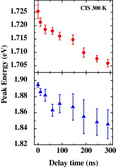
Figure 2 Peak energies of the two spectral components as a function of the delay time from the excitation moment.
Figure 3 shows the zero-delay TRPL spectra of CIS/ZnS NCs measured with various excitation densities changing by factors of 1–100. The observed blue-shifts of the peak energy with increasing excitation density, again, can be interpreted in terms of DAP recombination due to the decreasing contribution of distant DAPs. Therefore, we conclude that both of the spectral components originate from recombinations of electrons in donors and holes trapped in acceptors.
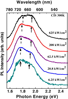
Figure 3 Zero-delay TRPL spectra from the 3-nm close-packed CIS/ZnS NCs, showing the evolution of the two spectral components with the excitation power density. The dashed and solid arrows indicate the peak energy positions of the low- and high-energy bands, respectively.
A CIS NC is built up by hexagonally close-packed atoms, composed of a central atom surrounded by a number of dense-packed shells that depend on the particle's size. The average core size of the CIS/ZnS core/shell NCs used here is ∼3 nm and the shell thickness ∼1 nm. Based on the reported lattice constants of CIS bulk crystal, a=0.5523 nm and c=1.1123 nm [8, 11], respectively, the total number of atoms in one particle is approximated to be ∼150 and the percentage of surface atoms is estimated to be ∼63% [20]. Furthermore, being a ternary compound, CIS contains more complicated lattice imperfections than, for example, binary II–VI semiconductors [9, 11]. Consequently, not only intrinsic defects but also surface defects act as potential fluctuations to localize charge carriers.
To study further the role of defects in the optical transitions in CIS/ZnS NCs, temperature-dependent emission bands were analyzed. The integrated emission of the two bands depicted as functions of temperature is shown in figure 4. Both show a decrease in the integrated PL intensity with decreasing temperature but in quite different ways. The integrated emission of the lower energy emission band is almost constant up to a temperature of 75 K and then shows an abrupt increase in the higher temperature region. In contrast, the integrated emission of the higher energy emission band demonstrates a gradual increase with increasing temperature. To explain this behavior, we suggest the existence of surface and intrinsic defect energy levels in NCs located below donor levels. For intrinsic defects, below a certain temperature the thermal energy is not sufficient for trapped electrons to be released from the defect states. Consequently, the integrated emission resulting from the radiative recombination of an electron in a donor level and a hole localized at the acceptor site becomes weaker with decreasing temperature. Subsequently, it becomes constant when the temperature is lower than a critical value that defines the lowest potential depth of the intrinsic defects, in this case approximately 6–7 meV. The situation is rather different, however, for the surface states, which possess various energy levels due to various types of coordination sphere. As a result, electrons trapped in surface defects are helped to escape from the trapping site to move to an emission site even at low temperatures. This process is thermally activated and consequently the integrated PL intensity increases with temperature. In the PL spectra, the higher energy emission band is therefore assigned to the surface-related defects.
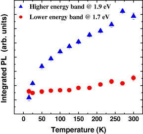
Figure 4 The integrated PL of the two emission bands as a function of temperature in which the integrated PL of the higher energy band and that of the lower energy band are shown by solid triangles and circles, respectively.
Figure 5 shows the typical decay curves at the emission energy of 1.69 and 1.94 eV at 300 K, which can be fitted qualitatively by bi-exponential functions. The faster decay time, changing from 12 to 80 ns on the emission energy, can be assigned to fast trapping processes of the non-radiative surface and intrinsic defect levels, respectively. The slower decay time varies from 120 to 390 ns, depending on the emission energy. Zhong et al [15] recently reported similar values for the decay time of optical transitions in CIS NCs. The decay times of the slow-decay components at the two emission energies of 1.69 and 1.94 eV are presented as functions of temperature in figure 6. The decay times are nearly independent of temperature at T >75 K and can be estimated to be 180 and 360 ns for the emission energies of 1.69 and 1.94 eV, respectively. We propose that these decay times are the radiative lifetimes of DAP in CIS NCs. In this temperature range, the thermal energy is high enough compared to the potential barriers of the defects. As a result, photoexcited electrons are almost not captured by the defects but released smoothly to the emission sites. On the other hand, the observed decay times increase sharply to values of several microseconds when the temperature is low enough. These long decay times can be described as 'population times', defined as the times that excited electrons need to escape from trap states and to go to the emission sites. Consequently, at low temperature, the trapping of electrons at defects not only lengthens the population processes of the emissive sites but also partly reduces the emission intensity.

Figure 5 The decay curves for the emission energies of 1.69 and 1.94 eV at 300 K, which are indicated by solid circles and triangles, respectively. The solid lines show the bi-exponential fitting curves.
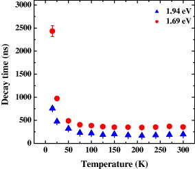
Figure 6 Decay times of the slower decay components at the emission energies of 1.94 eV (solid triangle) and 1.69 eV (solid circle) as a function of temperature.
4. Conclusion
In conclusion, we have studied the optical transitions in the 3-nm core CuInS 2/ZnS NCs by using a temperature-dependent TRPL technique with a variation in the excitation power density. Two emission bands were observed that evolve differently with the time elapsed from the excitation moment. Spectral characteristics of both observed emission bands demonstrate that they originate from DAP recombinations. The emission band at higher energy is assigned to surface-related defects in DAP recombination, while the one at lower energy is attributed to DAP inside the NCs. Below 50 K, the decay time is about four times longer than those at higher temperatures. With increasing temperature over 50 K, the decay time becomes much shorter and almost constant until 300 K. These results are explained in terms of charge carriers being released from traps to contribute to the emission. Therefore, the decay time observed at temperatures over 50 K means the radiative lifetime of DAP in CIS NCs.
Acknowledgments
The authors thank Dr L S Dang at Institut Néel for helpful discussions. The National Key Laboratory for Electronic Materials and Devices (IMS/VAST) and the CEA program 'Technologies pour la santé' (project TIMOMA2) are gratefully acknowledged for financial support.