
Abstract
Perpendicularly self-aligned TiO2 nanotube samples of size of 3 × 5 cm2 were fabricated by the electrochemical anodization method using a solution containing NH4F. Influences of the technological conditions such as NH4F concentration and anodization voltage were studied. It was found that NH4F concentration in the solution and anodization voltage significantly affect the diameter and length of a TiO2 nanotube. The diameter and the length of a TiO2 nanotube were observed and estimated by using scanning electron microscopy. It has shown that the largest diameter and the longest length of about 80 nm and 20 μm, respectively, were obtained for the sample anodized in a solution containing 0.4% of NH4F, under a voltage of 48 V. Photoluminescence spectra excited by laser lights having wavelengths of 325 and 442 nm (having energies higher and lower than the band gap energy of TiO2) was recorded at room temperature for the TiO2 nanotube arrays. An abnormal luminescence result was observed. It is experimental evidence that the manufactured TiO2 nanotube array is an expected material for hydrogen splitting from water by photochemical effect under sunlight as well as for the nano solar cells.
Export citation and abstract BibTeX RIS

Content from this work may be used under the terms of the Creative Commons Attribution 3.0 licence. Any further distribution of this work must maintain attribution to the author(s) and the title of the work, journal citation and DOI.
1. Introduction
TiO2 is one of the most intensively investigated compounds in material science due to its essential properties. It is a wide band gap semiconductor having band-edge positions appropriate for solar cell applications and for hydrogen generation by water splitting. It is also known as a non-toxic, environment friendly, corrosion-resistant material [1–4]. In particular, TiO2 nanocrystal is a very active photocatalytic material that has many powerful applications in biomedicine, environment technology and photochemistry. In 1972 Fujishima and Honda [5] reported an experimental result on water splitting for the first time using a TiO2 electrode illuminated with an ultraviolet light. In the 1980s and 1990s, many researches related to the use of TiO2 material for solar energy conversion were reported [6, 7]. Recently, Nguyen Van Hieu and Nguyen Bich Ha [8] have analyzed and discussed a large number of selected references and presented an essential review focused on the visible light responsive titania-based nanostructures and their applications in photoelectrochemical processes. For all of these applications, the specific surface area of TiO2 nanocrystal is essentially important. Nano forms of TiO2 such as nanoparticles, nanorods, nanowires and, in particular nanotubes may allow obtaining high efficiency photoelectrochemical devices. Since Iijima discovered carbon nanotubes in 1991, one-dimensional (1D) nanostructures have become a hot field of nanotechnology inspiring scientists and technologists to greater efforts in looking for new compounds [9]. The 1D structures provide unique properties, such as high electron mobility and very high specific surface area. Synthesis of 1D TiO2 may be achieved by various methods such as sol–gel, template-assisted, hydro/solvothermal and electrochemical anodization [10–13]. Using anodization in chromic acid electrolyte containing hydrofluoric acid, Zwilling et al [14] fabricated organized nanotube layers of up to about 500 nm in thickness with a considerable sidewall inhomogeneity. After Zwilling's report in 1999, several investigations using acidic fluoride-containing electrolytes confirmed that the sidewall inhomogeneity is associated with current fluctuations [15]. Macak et al demonstrated that the pH plays a crucial role in improving the tube layer thickness. Many authors successfully fabricated good hexagonally arranged nanotube layers with thickness of hundreds of micrometers using organic electrolytes such as ethylene glycol [16]. Recently, Tang et al [17] reported the result of manufacturing a micrometer long TiO2 nanotube using a high-viscous 0.5 wt% NH4F/glycerol solution. Schmulki completed a nice review on synthesis and applications of TiO2 nanotubes fabricated by electrochemical anodization. In this review the authors have dealt with the influences of the technological conditions such as the ratio of constituents in electrolyte and the applied voltage of anodization processing on morphology, structure of nanotube arrays fabricated by various techniques as well as their applications [18].
In this report, we present recent results of manufacturing the perpendicular self-aligned TiO2 nanotube arrays by using electrochemical anodization in an organic electrolyte containing NH4F at room temperature and of studying their optical properties.
2. Experimental
TiO2 nanotube arrays were grown by anodic oxidation at room temperature of high purity (99.7%) Ti foil in ethylene glycol solution containing 2 wt% deionized (DI) water and several different concentrations of NH4F for 3 h. Pt sheet was used as a counter electrode. The distance between the anode and cathode electrodes was kept of about 1.2 cm in all experiments. The anodization was carried out by varying the constant potential from 10 to 60 V. The anodization current was monitored using a Keithley 2000 multimeter. The experimental setup is shown in figure 1. Before anodization, Ti foil surface and Pt sheet were ultrasonically cleaned in ethanol for 20 min, in DI water for 10 min, and finally dried at 50 °C in air. After finishing the anodization process, TiO2 nanotube samples were immediately washed in DI water to remove residual ion F−, and then precipitates covering the surface of TiO2 nanotube arrays were removed by ultrasonication in ethanol for 30 s and subsequently dried in air. A typical anodized sample was annealed at 450 °C for 3 h (ramp 5 °C min−1) to completely transfer the TiO2 into anatase crystalline phase.
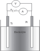
Figure 1. A modeling schema of the electrochemical anodization setup used to grow TiO2 nanotube arrays with the electrolyte containing ethylene glycol added NH4F of various concentrations and 2 wt% of deionized water.
Download figure:
Standard image High-resolution imageThe morphology of all the samples was evaluated by using a Hitachi SEM S4800. The crystalline structure and the optical absorption of typical TiO2 nanotube array membrane were investigated by using an x-ray diffractometer Siemen D 5000 with Cu-Kα radiation (λ =1.5406 Å) and a UV–Vis Cary 5000, respectively.
3. Results and discussions
In order to look for an optimal concentration of F− ions in electrolyte we have studied the dependence of morphology of the synthesized TiO2 nanotube arrays on the NH4F concentration in the range of 0.3–0.6 wt% as illustrated in figure 2.
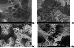
Figure 2. FESEM images of the TiO2 nanotube arrays synthesized under an anodization voltage of 45 V in the electrolyte containing ethylene glycol added 2 wt% H2O and various NH4F concentration of (a) 0.3, (b) 0.4, (c) 0.5 and (d) 0.6 wt% (the distance between two electrodes was 1.2 cm).
Download figure:
Standard image High-resolution imageUnder the same anodization voltage, the morphology and the size of TiO2 nanotube arrays obviously depend on NH4F concentration. It is clear to see the pores and the top of tubes in all the images. They confirm that all the used concentrations are in the intermediate range of fluoride concentration that will be more clearly explained later. Actually the nanotube arrays grown by using an electrolyte containing 0.4 wt% of NH4F has clear surface and homogeneous size of tubes in larger areas. In principle, these obtained results can be quantitatively explained as follows [19]. If the fluoride concentration is low (∼ 0.05 wt%) a stably compact TiO2 oxide layer is formed. If the fluoride concentration is high (about 1 wt%), the formation of TiO2 oxide is not observed. It is because all the formed Ti4+ ions immediately reacted with the ambient fluoride ions to form soluble [TiF6]2−. This reaction is electro-polishing the surface of TiO2 oxide so fluoride concentration acts as a factor to frustrate the formation of TiO2 tubes. For intermediate fluoride concentration (0.4 wt% in our case), the growth rate of TiO2 nanotube arrays is a consequence of the competition between the Ti4+ dissolution and the TiO2 tube creating by oxidation during the electrochemical anodization. Consequently, the growth rate of nanotube arrays and their size also depend on the anodization applied voltage. This dependence was studied and observed through the morphology of the nanotube arrays manufactured under various anodization voltages changed from 30 to 48 V (figure 3).
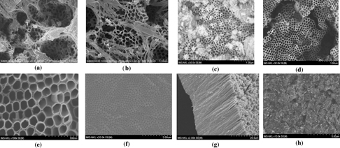
Figure 3. FESEM images of TiO2 nanotube arrays synthesized by electrochemical anodization under various voltages of 30 V (a), 40 V (b), 45 V (c) and 48 V (d) in a electrolyte containing ethylene glycol added 0.4 wt% of NH4F and 2 wt% of H2O (the distance between two electrodes is 1.2 cm). (e (top view), f (bottom view), g (cross-sectional view) and h (in a larger scale) are the images of the case when the distance between two electrodes is 0.6 cm).
Download figure:
Standard image High-resolution imageIt is clearly to see that the nanotube arrays grown under the low anodization voltages (smaller than 40 V in our case) do not exhibit good geometry. They are inhomogeneous in morphology and size. The geometry, morphology and size of the TiO2 nanotube arrays are much developed as increasing the applied voltage to 45 V. Especially, they reach the most homogeneous and nicest nanotube arrays when the applied anodization voltage are around 48 V. The best obtained nanotube array has the diameter and length of about 100 nm and 21 μm, respectively. Based on field emission scanning electron microscopy (FESEM) images with a highest resolution, the wall thickness of nanotubes has been evaluated as about 12 nm. Besides we can see that the tube wall is smooth. It implies that the water content is low as concluded in [20–21].
To understand the evolution of electrochemical anodization process, a typical J–t curve (current density–time dependence) has been plotted that presents the evolution of anodization current under two applied voltages of 45 and 48 V (figure 4). With applied anodization voltages lower than 45 V the anodic current continuously decreases in the whole time of anodization and behaves as a J–t characteristic curve similar to the compact oxide process that occurs in the case of the low fluoride concentration [18]. With higher anodic voltages of 45 and 48 V the J − t curves exhibit a continuous decrease with a flat maximal peak around 50 min. The shape of J–t curve is similar to the case of the intermediate fluoride concentration. The J–t curve in the case of the distance between Ti and Pt electrodes is 0.6 cm has been also shown in the figure 4 (the red one). It clearly exhibits a typical current evolution of the electrochemical anodization of Ti that consists of three parts. The initial part (from A to B in the J–t curve) with a decrease in anodization current is due to the increase in the thickness of the compact TiO2 oxide layer. Typically, the growth factor of many transition metal oxides including TiO2 is in the range of 2 − 4 nm V−1 [18]. Under a constant applied voltage U, the anodization driving field F = U/d decreases constantly, thus lowering the anodization current. Besides, the accumulation of fluoride ions caused by the anodization driving field also plays an additional role to prevent the move of the next fluoride ions to Ti foil's surface, and hence, decrease anodization current.
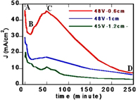
Figure 4. J − t (current density–time) curves of the anodization of Ti foil in an electrolyte containing ethylene glycol added 0.4 and 2 wt% of water under two voltages of 45 and 48 V.
Download figure:
Standard image High-resolution imageThe accumulation of fluoride ions is increased to reach the fluoride-rich state such that the fluoride ions penetrate the compact TiO2 oxide layer and dissolute Ti4+ ions from Ti foil under the anodization driving field, and consequently increase the anodization current to a maximal value at C point as seen in figure 4. The maximal point of anodization current is a consequence of the competition between the dissolution of Ti4+ ions and the formation of the soluble [TiF6]2− that causes the decrease of electrolyte conductivity. Theoretically, the electrolyte conductivity depends on the concentration of conducting ions and their mobility. So, in our case, the decrease of electrolyte conductivity may be due to the reduction of free fluoride ion concentration and its mobility caused by increasing the concentration of soluble [TiF6]2−. Therefore, the anodization current decreased when the electrochemical anodization time was prolonged, as seen in figure 4 (from C to D point). It implies that the morphology, geometry and tube homogeneousness of nanotube arrays can be developed by controlling the anodization time. The crystalline structure of TiO2 nanotube arrays was characterized by using x-ray diffraction (XRD). Figure 5 presents XRD patterns recorded at room temperature of the TiO2 arrays before and after annealed at 450 °C for 2 h. It was shown that the synthesized TiO2 array has smaller anatase crystal size compared to annealed sample. After annealing the anatase phase much developed and the nanocrystal size significantly increased. Figure 6 presents absorption spectra of the TiO2 synthesized nanotube array and the TiO2 film fabricated by spin coating from a solution containing TiO2 nanoparticle synthesized by sol–gel method.

Figure 5. XRD patterns of the TiO2 nanotube arrays: (a) the synthesized and (b) the annealed at 450 °C.
Download figure:
Standard image High-resolution image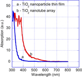
Figure 6. The absorption spectra of the TiO2 nanoparticle thin film synthesized by a hydrothermal method (a) and the as-synthesized TiO2 nanotube array (b).
Download figure:
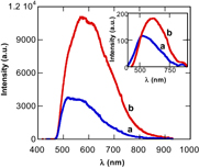
Standard image High-resolution imageFrom figure 6 we see that the band gap energy of TiO2 nanotube array is smaller than that of the TiO2 nanoparticle film. Besides, the TiO2 nanoparticle film has a sharp absorption edge, otherwise the absorption band edge of the nanotube arrays is not sharp and, furthermore, they have long tails extended to 2.4 eV. It is supposed to be related to the oxygen deficiency in nanotube material. It was known that, in the TiO2 with oxygen deficiency, Ti3+ states have appeared on demand of the electrical neutralization and they have contributed as impurity states locating below conduction band of about 0.1–0.8 eV [22]. The obtained shift of absorption band edge and the long tail in absorption spectra turn on the response of TiO2 nanotube arrays to the visible light and open the possibility of using TiO2 nanotube in photocatalysis. In addition, for greater understanding, the room temperature photoluminescence excited by laser beams of 325 and 442 nm in wavelength for both the synthesized and annealed arrays are shown in figure 7. It was found that the samples weakly emit when excited by a laser beam of 325 nm in wavelength. In contrast, both samples strongly emit when excited by a laser beam of 442 nm. A similar photoluminescence result was observed for the Cu-doped TiO2 nanocrystal particles reported in our previous work [23]. It was reported that the Cu-doped TiO2 nano-particles with grain size of about 5–6 nm did not completely emit when excited by a laser light of 325 nm, but weakly emitted when excited by a laser light of 442 nm. A two-steps model as reported in [23] was used to explain the photoluminescence results and suggested that the obtained luminescence result is an experimental evidence to confirm the present of energy levels in the band gap of TiO2 nanotube arrays which improve ability to use the TiO2 nanocrystals in solar cells and water splitting application.
Figure 7. Photoluminescence spectra of the nanotube arrays excited by laser beams of 442 and 325 nm (inset): (a) the as synthesized and (b) annealed at 450 °C for 2 h.
Download figure:
Standard image High-resolution image
The difference between the TiO2 nanoparticles and TiO2 nanotube arrays is that the nanotube arrays have a weak emission when excited by 325 nm laser beam while the nanoparticles have no emission. It may be concerned with the wall size and the length of the nanotube being 12 nm and 21 μm, much larger than grain size of nanoparticles (5–6 nm) [23]. The nanotube arrays more strongly emit when excited by 442 nm laser beam. It is supposed to be related with the presence of the energy levels in the band gap of TiO2 as in the case of nanoparticles doped with Cu.
4. Conclusions
TiO2 nanotube arrays were successfully manufactured by electrochemical anodization on Ti foil. The array grown under a driving field of about 80 V cm−1 in an organic electrolyte containing ethylene glycol added 0.4 wt% of NH4F and 2 wt% of H2O has the best morphology, homogeneous distribution of tubes with the diameter and length of about 80 nm and 21 μm, respectively. The wall thickness of the tubes changed from 9 to 12 nm for the synthesized and annealed samples at 450 °C, respectively. The TiO2 nanotube arrays have the absorption edge around 3 eV with a long tail of about 0.8 eV below the conduction band that is supposed to be related to the oxygen deficiency and it is a reason for the higher electronic conductivity of TiO2 nanotubes. An abnormal phenomenon in photoluminescence of TiO2 nanotube arrays was observed when excited by two laser lights having energies higher and lower than the band gap of TiO2. It is an experimental evidence to believe that TiO2 nanotube arrays are an expected photocatalytic material responsive to the visible light and applicable for photocatalysis, solar cells and water splitting under sunlight.
Acknowledgments
This work was performed under the financial support by the project of VAST under Grant number of VAST03.08/12-13. The authors are grateful to Professor Academician Nguyen Van Hieu for his support to open the nanomaterials used in the energy conversion including solar cells and water splitting, and also to the Key Laboratory of Electronic Materials for the technical support in FESEM and XRD measurements.