
Abstract
Processing of group III-nitride materials such as AlN in the form of photonic crystals or microdiscs opens new perspectives for basic cavity quantum electrodynamic studies or the development of novel devices operating in the ultra-violet range. These devices can be either passive or active by embedding self-assembled GaN quantum dots. We review the recent progress achieved in the field of nitride-based microresonators for UV nanophotonics.
Export citation and abstract BibTeX RIS

Content from this work may be used under the terms of the Creative Commons Attribution 3.0 licence. Any further distribution of this work must maintain attribution to the author(s) and the title of the work, journal citation and DOI.
1. Introduction
The field of ultra-violet (UV) nanophotonics is attracting considerable interest from the solid-state and photonics communities. The control of optical emission by artificially patterned materials has been thoroughly investigated in the visible or near-infrared spectral range. Both the control of the recombination rate and control on the spatial distribution of emitted light are enabled by patterning at the micro and nanoscales. The transposition of these concepts in the UV opens new perspectives to enhance the performance of devices at short wavelength, either in the UV-A (400–320 nm), UV-B (320–280 nm) or UV-C (280–200 nm) ranges. The field is becoming even more attractive thanks to the progress achieved in the growth and processing of nitride materials. The group III-nitrides are obviously a preferred choice for UV nanophotonics. A material such as aluminum nitride (AlN) exhibits a very large band gap (6.2 eV at room temperature) and is thus transparent in the UV. The nitride band gap can be tuned by growing heterostructures with GaN or alloys containing Al and In. Active materials such as quantum wells or self-assembled quantum dots can be embedded in AlN, thus opening the route to fabricate light-emitting devices or lasers. AlN layers can be grown on sapphire and silicon carbide substrates but also on silicon substrates. The growth on silicon is a key advantage to develop a wafer-scale nitride-based platform for nanophotonics. Besides being a very cost-effective substrate, selective chemical etching between nitride and silicon allows one to easily fabricate self-supported membranes, a feature not so easily achieved with substrates such as SiC where photoelectrochemical etching steps must be implemented. Even if the refractive index of AlN is relatively small (2.15 in the near-UV range), both photonic band gaps and high quality factor resonators can be obtained with membrane-type photonic crystals. The membrane approach maximizes the refractive index difference between air and material where light is mostly confined and at the same time provides symmetric structures along the vertical direction, thus minimizing coupling between transverse electric (TE) and transverse magnetic (TM) polarizations and in fine losses.
Numerous types of nanophotonics structures have been investigated to date using group-III nitride layers. The patterning of nitride materials can lead to enhanced extraction efficiency for light-emitting devices [1] and represents a major challenge for improving the luminance of the diodes. Photonic crystal and microdisc lasers have been demonstrated with InGaN quantum wells as active materials [2, 3]. In the latter cases, the structures were grown on sapphire or GaN substrates. The quest for microresonators is motivated by the fact that the achievement of high quality factor and small mode volume cavities enhances the linear and nonlinear light–matter interactions: this can for example translate into a decrease of lasing threshold or the possibility to obtain a nonlinear response for very small input power or energies. Moreover, nitride materials are non-centrosymmetric materials and exhibit a large second-order nonlinear susceptibility [4]. This presents thus a significant interest for harmonic generation. Besides, photonic crystals offer new approaches to achieve quasi-phase matching and efficient harmonic conversion [5, 6] or to study nanocavity-based self-frequency conversion lasers [7].
A way to develop nanophotonics with nitride materials, i.e. in the UV spectral range, is to fabricate structures from AlN layers. AlN-based nanophotonics has thus emerged as a new domain for UV applications. The challenges are significant: going to shorter wavelength requires downsizing the typical parameters for processing (periodicity, hole sizes, etc). Meanwhile, the sensitivity to scattering increases significantly at short wavelength leading to higher losses. Large efforts have thus been devoted to the optimization of the design and the fabrication processes of small AlN-based resonators. In the following we will review the latest advances in this domain, either for photonic crystals or microdiscs.
2. Fabrication of AlN microresonators
The processing steps to obtain nitride resonators greatly depend on the host substrate. The host substrate should allow the growth of high quality material and at the same time the release of suspended structures for photonic crystals. One of the first demonstrations of AlN photonic crystal resonators was obtained with a layer grown on a silicon carbide substrate [8]. Silicon carbide has a low lattice mismatch with AlN. Meanwhile, there is no easy processing step to release a membrane in this case. To circumvent the problem, the authors have used a technique of photoelectrochemical etching that relies on the accumulated stress in the layer. One of the drawbacks of this technique is the bending of the epitaxial layer. The second drawback is the deterioration of the AlN interface due to the interaction of the fluorhydric acid with nitrogen-terminated interface. An alternative approach has been proposed and relies on the use of layer transfer [9]. The epilayer is transferred by wafer bonding on a silicon substrate while the silicon carbide substrate is removed by plasma and chemical etching. The transfer on silicon offers the advantage to facilitate the underetching of the membrane. The advantage of a silicon substrate cannot be restricted to the membrane release. There is a major interest to integrate UV nanophotonics on silicon, due to the low cost of the substrate and more importantly due to the versatility offered for processing, integration of complex architectures and the compatibility with silicon microelectronics. UV nanophotonics is an additional toolbox in the fast-growing field of silicon photonics.
We have developed two main approaches to fabricate nitride photonic crystals on silicon, either bottom up or top down. In the bottom up approach, the first step is to pattern the silicon. Typically, the lattice periodicity a is in the range of 150 nm and the ratio between hole radius and lattice parameter r/a is around 0.25–0.3. The patterning is performed using standard silicon processing combining electron lithography and silicon plasma etching. In a second step, the nitride is grown on top of this patterned silicon substrate by molecular beam epitaxy [10]. One obtains a conformal growth that replicates the silicon pattern. The advantage of this approach is that it does not require the etching of the nitride material. As shown in [10], quality factors up to 1800 at 425 nm can be obtained by this approach with AlN photonic crystals.
The second approach is more conventional and is based on a top-down scheme [11]. It is the one that is mostly used for near-infrared photonic crystal fabrication. Figure 1 schematically shows the different steps. The AlN epilayer is first grown on silicon by molecular beam epitaxy. A SiO2 layer is then deposited by plasma enhanced chemical vapor deposition and will be used as a hard mask. After photoresist deposition and electronic lithography, the SiO2 layer is etched by reactive ion etching. The pattern is then transferred into the nitride by chlorine-based inductively coupled plasma (ICP) etching, using a mixture of Cl2, BCl3 and Ar gases. The SiO2 layer is removed using fluorhydric acid and the suspended-membrane is then released using XeF2 etching. In this approach, there is a direct etching of the nitride material. This step is critical as the optical properties are directly dependent on the lithography and etching performances: homogeneity, verticality of the side walls, roughness and regularity. The nitride thickness h to etch depends on the targeted wavelength with typically a ratio h/a = 0.6 for an AlN membrane. Going to short wavelength with lattice periodicity of 130 nm or lower remains challenging for fabrication.
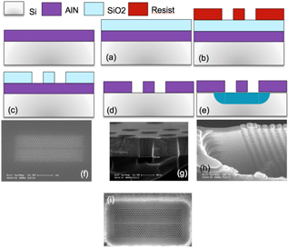
Figure 1. Schematic presentation of the fabrication of a nitride membrane photonic crystal using a top-down approach. The successive processing steps are: (a) deposition of SiO2 hard mask; (b) deposition and patterning of electronic resist; (c) pattern transfer in the SiO2 hard mask by reactive ion etching; (d) pattern transfer in the aluminum nitride layer by chlorine-based ICP etching followed by the removal of the SiO2 hard mask; and (e) underetching of the silicon substrate by exposure to XeF2. The scanning electron microscopy images show images of the photoresist pattern (left—(f)), a cross-section after ICP etching (middle—(g)) and a tilted view after substrate removal showing the high quality of the bottom surface of the AlN layer (right—(h)). The bottom picture (i) shows a top view of the fabricated structure.
Download figure:
Standard image High-resolution image3. Optical properties of microresonators
3.1. Photonic crystals
There are several ways to probe the photonic crystal optical properties. The standard far-field spectroscopies rely on the coupling between cavity modes and free-space propagating modes. Modes can thus be identified in reflection or transmission geometries. In the UV, the lack of a convenient tunable optical source makes this transmission or reflection far-field approach less attractive. The use of internal photoluminescence either from the bulk [12] or from quantum dots [13] is by far more convenient. The quantum dots can provide a spectrally broad internal source with a low absorption that limits quality factor degradation. The dot emission can be coupled to modes with different parities which are not easily addressed in standard in-plane transmission geometries. Moreover, dense GaN quantum dots embedded in thin AlN layers can exhibit a strong emission at room temperature [14], thus representing very convenient internal emitters.
Figure 2 shows a typical room-temperature photoluminescence spectrum of an AlN width-modulated waveguide cavity. The active structure consists of a 35 nm thick buffer layer of AlN, first grown on a Si substrate, followed by the growth of one plane of GaN QDs, which is then capped by 35 nm AlN. The investigated cavities are width-modulated cavities defined in a W1 waveguide following the A1 design proposed in [15]. A W1 waveguide corresponds to one missing row of holes along one direction. Thirty holes around the cavity center are displaced from their nominal position by a distance d (12 nm for the four holes at the cavity center and a fraction of this value around in this example). The cavities are probed at room temperature by microphotoluminescence using a focused continuous wave (CW) laser (spot size ∼ 1 μm) at 244 or 266 nm. The excitation laser was focused through a microscope objective (numerical aperture 0.4) on the center of the pattern (i.e. at the cavity location) and the photoluminescence is collected through the same objective. The photoluminescence was analyzed by a grating spectrometer and detected by a UV-enhanced liquid-nitrogen cooled Si charge coupled device detector.
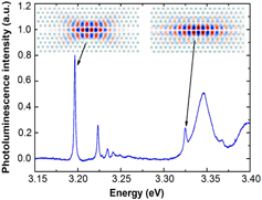
Figure 2. Room temperature photoluminescence spectrum of an AlN width modulated waveguide cavity. The maximum lateral hole displacement at the cavity center is 12 nm. The lattice periodicity is 170 nm. The insets show the profile of the Hz field amplitude for the fundamental even and odd cavity modes, experimentally observed at 3.196 and 3.325 eV, respectively. The mode profiles are obtained by three-dimensional finite difference in time domain calculations.
Download figure:
Standard image High-resolution imageThe studied cavity in figure 2 has a lattice periodicity a = 170 nm and r/a ratio of 0.27. At low energy, a series of resonances is observed between 3.19–3.25 eV. The lowest resonance at 3.196 eV (388 nm) corresponds to the fundamental mode of the cavity. The second resonance at 3.225 eV is also a cavity mode. Mode imaging reveals that this mode is also located at the cavity center with a small lateral extension [16]. The modes between 3.23 and 3.25 eV correspond to one-dimensional waveguide modes. Spatially, the maximum of these modes is not found at cavity center and is expected to be spatially delocalized along the waveguide. They turn out to be localized by disorder induced by fabrication [16]. At higher energy, one also observes a cavity mode at 3.325 eV but with an odd symmetry for the Hz or Ey field amplitude with respect to the waveguide axis (see inset that shows the mode profile calculated by three-dimensional finite-difference time-domain (3D-FDTD) method). We did check that the resonance energy of the cavity modes can be controlled by the lateral displacement d of the holes [11].
The cavity presented in figure 2 has a quality factor of 4400 at 389 nm. Modeling by three-dimensional finite difference in time domain indicates that the theoretical Q factor of the fundamental mode of this width-modulated cavity is around 10 000. There is thus a significant difference: several parameters can explain the discrepancy. A small roughness of the vertical sidewalls of the holes can induce some scattering and provide some additional losses. The verticality of the holes is quite good, but even a small angle can induce some TE–TM coupling. As there is no photonic band gap in TM polarizations, it leads to additional loss mechanisms. The deviation of the hole positions from their nominal positions as well as a deviation in their size and forms are also likely to degrade the quality factors. All these parameters need thus to be optimized, in order to achieve better quality factors. In the literature, similar results have been reported. Sergent et al [17] have demonstrated a Q factor of 5000 at 380 nm in a so-called nanobeam cavity fabricated in a free-standing ridge waveguide. The same group has reported a Q factor of 6000 at 399 nm by using a layer transfer approach [9]. Layer transfer allows the use of processed AlN without photoelectrochemical etching. The progress with layer transfer has been attributed to the suppression of the cavity bending and surface roughness of the nitrogen-face AlN. Vico Trivino et al [18] have reported Q factors of 5200 at 420 nm at low temperature in a L7 cavity fabricated in a AlN/GaN/InGaN vertical stack initially grown on silicon.
One of the challenges of UV nanophotonics is to go to shorter wavelengths. There are several ways to tune the resonance emission: decreasing the lattice parameter; and increasing the air hole ratio or decreasing the slab thickness. Figure 3 shows examples of photoluminescence spectra at shorter wavelength obtained by reducing the lattice parameter (150 and 130 nm). The r/a ratio is also increased. Experimentally, resonances at 330 and 290 nm are clearly observed. One of the drawbacks is the decrease of the quality factors. One contribution to this decrease is the quantum dot absorption involving excited levels that is significantly larger than the quantum dot absorption between ground states. Such a decrease when going to short wavelengh was also observed in [17], and the achievement of high quality factors at very short wavelength is still a challenge.
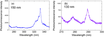
Figure 3. Examples of photonic crystal resonances at short wavelength obtained with AlN width modulated waveguide cavities (75 nm thickness). (a) 150 nm lattice parameter and (b) 130 nm lattice parameter. The horizontal scale is different between (a) and (b). Resonances down to 290 nm can be obtained. Quality factors of 2300 were obtained at 358 nm for a hole displacement of 6 nm (not shown) [11].
Download figure:
Standard image High-resolution imageThe motivation to obtain high quality factor is multifold. A high quality factor can increase the radiative recombination rate through the Purcell effect. The Purcell factor Fp is given by

assuming a perfect spatial and spectral matching between the emitter and the cavity linewidth and a narrow emitter linewidth. Veff is the cavity effective modal volume. For a width-modulated waveguide cavity, the modal volume is around 2.2(λ/n)3. Typically, ideal Purcell factors around 200 are predicted for cavities as presented above with resonances around 400 nm and Q factors around 5000. More interesting is the possibility to achieve a UV nanolaser with GaN quantum dots inside the resonators. If we consider the rate equations and take into account the Purcell effect, the lasing conditions can be described by a parameter ξ with

where Nt is the number of quantum dots within the modes both spectrally and spatially, β the spontaneous emission coupling factor, τe the average spontaneous emission rate of the dots in the mode and γc the photon escape rate out of the cavity [19]. Apart from the quantum dot density, the two main parameters which control the onset of lasing are the cavity photon lifetime that can be increased by increasing the Q factor of the cavity and the spontaneous emission rate of the quantum dots. It is well known that the spontaneous emission rate of GaN quantum dots depends on the emission wavelength [20]. For quantum dots emitting around 3 eV, the Stark effect that separates electron and hole wavefunctions is very strong and leads to recombination lifetimes around 200 ns. This value can be decreased down to 0.5 ns for quantum dots emitting around 4.1 eV (300 nm). The combination of resonators and quantum dots emitting around 400 nm is not sufficient to achieve lasing in view of the quality factors demonstrated (ξ ∼10−4). One of the main issues for achieving lasing with AlN resonators and quantum dots will be to fabricate resonators with high quality factors at very short wavelength, thus allowing the use of quantum dots with shorter radiative lifetimes.
3.2. Microdiscs
Another approach to obtain microresonators is to fabricate microdiscs. The whispering gallery modes can support high quality factors and small modal volumes. Numerous demonstrations of nitride microdiscs have been reported. Room temperature microdisc lasers with InGaN/GaN active layers have been reported in the blue range at 430 nm [3, 21]. In the latter cases, the growth was carried out on sapphire substrates. We have recently reported high-quality nitride-based AlN microdisc cavities with GaN quantum dots. The samples were directly grown on a silicon substrate. Figure 4 shows a room temperature photoluminescence spectrum of an AlN microdisc on silicon [22]. Quality factors as large as 7300 at 410 nm for disc diameters of 5 μm (5000 for 2 μm diameter) have been obtained. The elements limiting the quality factor have been identified as the absorption in the silicon post and the absorption in the optical active area. It is thus possible to obtain quality factors in the same range in the UV either for photonic crystals and microdiscs. Whispering gallery modes with Q factors up to 1400 at 340 nm have also been observed with AlN microdiscs grown on a silicon carbide buffer layer on a silicon substrate [23]. The undercut of the microdisc was obtained by CF4 reactive ion etching. The main loss mechanisms were identified as light scattering at the sidewalls as well as scattering at the top and bottom surface. It is interesting to note that these microdiscs did contain non-polar quantum dots, which is an advantage if we consider the radiative recombination lifetime. More recently, the same group reported microdiscs with quality factors up to 5000 at 310 nm in similar structures [24]. This paper also reported a nonlinear behavior of the whispering gallery modes at large optical excitation power, which the authors attribute to lasing. We nonetheless note that in this work the quantum dot background luminescence also behaves nonlinearly in the same power range (most probably due to filling of quantum dot excited states). In the experimental data presented in [24], it is thus not clear whether the nonlinear behavior of the optical modes stems from lasing, from QD excited state filling or from a combination of both effects.

Figure 4. Room temperature photoluminescence of a 5 μm diameter microdisc. The inset shows a zoom around one resonance, highlighting the high Q factors that can be achieved. Both TE and TM polarized modes contribute to the resonances. The second inset (b) shows a scanning electron microscopy image of an AlN microdisc and its silicon post. The disc diameter is 2 μm. The disc contains AlN quantum dots as internal emitter.
Download figure:
Standard image High-resolution image4. Toward a nitride photonic circuit platform
One of the driving forces in nanophotonics is the development of complex photonic circuits which can combine several functions of emission, routing, modulation, detection and delay to control the propagation of light. One of the interesting features of these planar photonic platforms is the versatility that they can offer and the heterogeneous integration with the electronic circuitry. For that purpose, a nitride photonic platform developed on silicon certainly presents major advantages. A current trend is thus the demonstration of integrated photonics on silicon with nitride materials and photonic crystals. This trend, which consists in mixing the benefits of III–V semiconductors and silicon, is not limited to the blue or UV range. There is also an interest to develop such a platform in the near infrared. Nitride materials are wide band gap semiconductors and we expect that two-photon and three-photon absorption will be strongly limited in these materials for pump wavelengths above 800–900 nm. In silicon, two-photon absorption and the consequent free carrier absorption represent severe loss mechanisms which can in some cases mask the nonlinear effects that were initially targeted. The nitride platform is also an attractive solution for harmonic generation at different wavelengths from the near-infrared to the UV [25], the photonic crystals bringing more flexibility to achieve quasi-phase matching [6]. Integrated optomechanical resonators are also very promising due to the large piezoelectric coefficient of AlN [26]. There is thus a lot of potential behind these aluminum nitride photonic circuits, which can enable the coverage of a much extended spectral range.
A first demonstration of nitride photonic crystal platform has been reported recently [27, 28]. GaN self-supported structures including suspended waveguides by nanotethers, and photonic crystals were demonstrated on AlN/GaN epilayers grown on silicon. The planar geometry is similar to the one previously demonstrated on silicon-on-insulator or on diamond [29, 30]. Quality factors up to 5400 have been measured at 1611 nm. It is interesting to note that these Q factors are not significantly different from those achieved in the UV. One can certainly expect a lot of progress in the near future but this fact highlights the difficulties inherent to nitride processing. Going to longer wavelength requires thicker materials and the etching of thick slabs such that high quality becomes a real challenge. In the same near-infrared spectral range, AlN nanobeam cavities were demonstrated using AlN-on-insulator substrates [26, 31]. One of the drawbacks is that the sputtered AlN used in the latter works has a random crystalline orientation. It can, however, lead to wafer-scale photonic circuitries with very large quality factors up to 146 000 at 1530 nm [31]. This high quality factor was obtained in a one-dimensional nanobeam cavity, i.e. in a system where lateral confinement is provided by the suspended waveguide instead of the two-dimensional photonic band gap. This type of design is known to be less sensitive to disorder than two-dimensional photonic crystal cavities. Nonetheless, this result highlights the potential of AlN-based cavities for nonlinear studies in the near-infrared.
Figure 5 shows an example of key elements for a planar photonic platform in the near infrared fabricated from an AlN layer on silicon. The AlN is epitaxially grown by molecular beam epitaxy on silicon. Its thickness is 350 nm, i.e. close to λ/2n. The structure consists of a combination of suspended waveguides and suspended photonic crystal membranes. The photonic crystal is a W1 waveguide. The injection waveguides have a width equivalent to the width of the W1 waveguide. Coupling between the suspended ridge waveguides and the photonic crystals is engineered in order to maximize the coupling ratio. The waveguides are suspended by nanotethers. One of the challenges for this type of structure is to manage the residual stress present in the AlN layer that can lead to the breakdown of the whole structure. The size of the tethers has thus to be scaled accordingly. It is interesting to note that mm-long suspended structures can be obtained by this approach. Light can be injected directly in the waveguide or through a tapered waveguide. This type of platform can obviously be transposed to shorter wavelengths by adapting the parameters, i.e. layer thickness and lattice periodicity. This platform on silicon represents a very strong interest for the study on nonlinear photonics from the near-infrared to the UV and to take advantage of the versatility offered by photonic crystals to engineer light propagation.

Figure 5. Example of AlN photonic circuits for the near infrared. The AlN layer is 350 nm thick. Waveguides and photonic crystals are self-supported after underetching the silicon substrate. (a) View of the suspended access waveguide and a short taper. In the next processing step, the sample will be cleaved through the square around the waveguide termination. Light can thus be coupled efficiently into the waveguide with a lensed-fiber. (b) Zoom around the same area. (c) Image of the suspended waveguide and the photonic crystal. (d) Zoom of the coupling area between photonic crystal and waveguide.
Download figure:
Standard image High-resolution image
5. Conclusion
In conclusion, we have reviewed the recent achievements in the field of AlN nanophotonics using either photonic crystal or microdiscs. Significant progress has been achieved in the fabrication of AlN microresonators with optical resonances at short wavelength. Resonators with high quality factors are now routinely obtained in the 380–400 nm spectral range. One of the next challenges will be to obtain similar results at shorter wavelengths, down to 300 nm. This should allow one to achieve quantum dot lasing with these microresonators and study quantum electrodynamic effects in the UV. Besides, a new field has recently emerged with the demonstration of nitride photonic circuit platforms on silicon. The planar geometry combining suspended waveguides, photonic crystals and ring resonators opens new perspectives to achieve complex light manipulation on chip from the near-infrared to the UV.
Acknowledgment
This work was supported by the RENATECH network, the Labex GANEX and Region Ile de France (C'Nano 2011 Nanoetch project). This work was also partly supported by Agence Nationale de la Recherche under QUANONIC convention (ANR-13-BS10-0010-03). We thank Sylvain David, Sylvain Sergent, Meletis Mexis, Juanebur Rashid and Diane Sam-Giao for their earlier contributions to this work during their PhD, post-doc, or stay at IEF. We thank Jean-Yves Duboz for his support and fruitful discussions.