
Abstract
In this paper a simulation study is used to investigate the RF performance of surrounding gate (SRG) MOSFET. The effect of nonsymmetrical gate structure caused by non- ideality in fabrication process has also been taken care into consideration. The important RF figure-of-merits such as unity-gain cut-off frequency fT and maximum operating frequency fMAX are studied with the help of a 2D device simulator. Their trends related to the variation of different design parameters such as radius, oxide thickness, gate length, and doping along the downscaling have also been reported.
Export citation and abstract BibTeX RIS

Original content from this work may be used under the terms of the Creative Commons Attribution 3.0 licence. Any further distribution of this work must maintain attribution to the author(s) and the title of the work, journal citation and DOI.
1. Introduction
Physical dimensions of metal oxide semiconductor field-effect transistor (MOSFET) devices have been continuously scaled down over the past four decades [1]. As the dimensions of MOSFET device are continuously scaled down, many physical effects known as short channel effects (SCEs) play major roles in determining the performance of scaled devices.
To continue the rapid cadence of MOSFET downscaling and to push scaling beyond the limits foreseen by conventional planar device structure, the introduction of new technologies is being explored. Among various possible alternatives to traditional silicon planar MOSFET structures that are being explored is the surrounding gate nanowire MOSFET. The surrounding gate nanowire transistor exhibited better performance than single-gate device, and so is a possible candidate for extending the evolution of complementary metal oxide semiconductor (CMOS) technology.
Recently, due to the perfect geometry and electrostatics of the gate-all-around structure, surrounding gate metal oxide semiconductor (SRG MOS) devices have attracted much attention recently and emerged as the most promising devices in continuing the cadence in CMOS downscaling by showing their efficacy in preventing short-channel effects [2–8].
For digital logic applications, scaling challenges include control of leakage currents, immunity against SCEs, increasing drain saturation current while reducing the power supply voltage, and maintaining control of device parameters (e.g., threshold voltage) across the chip and from chip to chip. For analog/mixed-signal/RF applications, the additional scaling challenges include linearity, low noise performance, high unity-gain cut-off frequency, high intrinsic gain and good transistor matching. With the evolution of SRG MOSFET scaled down to deca-nanoscale regime, the high-frequency capabilities of the transistor have reached the GHz regime, compatible with typical radio-frequency (RF) circuit applications. Therefore, accurate RF performance modeling along the downscaling is a prerequisite for the development of low noise RF integrated-circuit (IC) design using multiple-gate MOSFET technologies. So far, many works in fabrication and simulation on the band structure and transport properties, impacts of process variation, and the design optimization for logic/digital applications [2–8] of SRG MOS devices have been done. However, few studies on the RF performance of SRG MOS device have been reported [9, 10].
Furthermore, the advancement in CMOS technology has made it also attractive for system-on-chip (SoC) applications where the RF circuits dominated by bipolar technology over the years are replaced by MOS devices without making compromise on RF performance parameters such as unity-gain cut-off frequency, maximum operating frequency etc, in order to reduce the cost and improve the performance of RF circuits. Therefore, new device structures such as surrounding gate MOSFET need to meet the RF requirements, which is one of the key building blocks of any SoC design. In order to realize the low-cost RF mixed signal CMOS SoC, the device structure of RF-CMOS should be the same as that of logic CMOS so that no additional fabrication steps are necessary. Because differences exist in the optimization of logic and RF CMOS device structures, there has been a concern for every scaled CMOS generation, whether such low-cost RF mixed CMOS devices can satisfy the RF requirement for high-performance RF application, such as cellular phones. Owing to its importance in the deca-nanometer regime and challenges in developing technologies, there is a strong need for evaluation of RF performance characteristic trends along the downscaling for the low noise, RF IC design. Accurate extraction of parasitic is critical in RF circuit simulation and accurate modeling of intrinsic device. The extraction of gate resistance is also particularly important. While accurate modeling of the MOSFETs is a critical requirement for circuit designs, the RF behavior along the downscaling and the physics that is expected to be affected seriously by device parasitic have not been reported much and are also lacking attention.
The unity-gain cut-off frequency (fT) and maximum operating frequency (fMAX) are considered as the most important RF figure-of-merits (FOMs). In an SRG MOS device, because of the higher mobility, transconductance can be higher, which gives more current gain and allows a higher operating frequency. Therefore, SRG MOS nano-scale devices have a big potential for RF and microwave applications. Therefore, it is crucial to confirm the suitability of sub-100 nm SRG MOSFET for RF adaptation.
In spite of the several benefits, the major issue that remains in the SRG MOSFET is its susceptibility to process variations that affect the eventual circuit performance. Among them, the most significant concern that gives rise to variations in the SRG device performance is the gate-source/drain overlap. The gate-source/drain overlap would affect several device properties of SRG MOSFETs. The viability of gate-source/drain overlap as a design parameter, in addition to typical device design parameters such as gate length, radius of nanowire etc, is investigated in terms of the sensitivity of SRG RF performance to the variations of process parameters that influence overlap properties. Therefore, in this paper, for the first time, a simulation study is used to investigate the RF performance of surrounding gate (SRG) MOSFET considering the effect of nonsymmetrical gate structure caused by non-ideality in fabrication process. The variation of important RF FOMs such as unity-gain cut-off frequency fT and maximum operating frequency fMAX is studied with the help of a 2D device simulator; and their trends related to the variation of different design parameters such as radius, oxide thickness, gate length, and doping along the downscaling are also reported.
2. Device structure and simulation
The schematic view of the simulated SRG MOSFET is shown in figure 1. N-channel device structure are created and simulated by 2D device simulator ATLAS [11] with the device parameters taken according to ITRS roadmap [12]. The simulation involves CVT model along with Shockley–Read–Hall (SRH) and Auger recombination models for minority carrier recombination. We also adopt CONMOB model for low field mobility related to doping density and FLDMOB model for high field velocity saturation depending on parallel electric field in the directions of current flow. Gummel's method along with Newton's method used to solve the equations involved in conventional drift-diffusion model is adopted for carrier transport. An ac small signal device simulation is performed over a wide frequency range, to compute the various RF-FOMs parameters with an applied frequency of 1 GHz. The drain-to-source voltage VDS = 1 V and thickness of oxide tOX = 2 nm are considered for all the simulations.

Figure 1. Schematic diagram of SRG MOSFET showing gate underlap and overlap.
Download figure:
Standard image High-resolution imageRF TCAD simulation is performed to examine the impact of variation of device parameters on small signal RF FOMs including unity-gain cut-off frequency fT representing the general RF behavior of a device and maximum operating frequency fMAX denoting RF power performance.
The approximate value of unity-gain cut-off frequency fT and maximum operating frequency fMAX is given by [13]
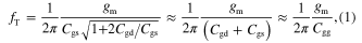
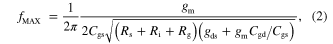
where Cgs, Cgd and Cgg are the gate-to-source, gate-to-drain and total gate capacitances, respectively, including fringing and overlap capacitances, gm and gds are the transconductance and output conductance, Rg, Rs and Ri are the gate, source and channel resistance (in series with Cgs), respectively, taking into account the distributed nature of the MOSFET. As inferred from equation (1) fT depends on the ratio of gm and total gate capacitances and from equation (2) that fMAX depends on the source/drain and gate parasitic resistances, and the miller capacitance to gate ratio Cgd/Cgs. Therefore, it is also evident that both the FOMs (fT and fMAX) are greatly influenced by geometrical parameters and parasitic capacitances have to be as low as possible to achieve a higher fT and fMAX values to meet the desired RF requirements.
There are three primary important parasitic components determining the RF FOMs, namely: (i) gate resistance, (ii) source/drain (S/D) series resistances, and (iii) gate parasitic capacitances. In an SRG MOSFET, fringing capacitance Cfr and overlap capacitance Cov are the dominant parasitic capacitances. Parasitic resistance in silicon-nanowire-tube (SNWT) mainly consists of the resistance of the gate regions and the contact resistance. In designing radio-frequency CMOS circuits approaching gigahertz frequencies, the gate resistance plays a major role and needs to be added to the intrinsic gate-engineered MOSFET simulation model to predict the device behavior at a high frequency. To reduce gate resistance, sometimes multi-finger are used or it can also be reduced by a factor of 10 with a silicide process, and even more with a metal stack process. We use the typical gate thickness in our analysis because, though reducing thickness of gate electrode metals reduces outer fringing capacitance Cof, it, however, considerably increases the gate resistance. This will significantly affect the performance as well as the power consumption in a circuit. Molybdenum is considered to be a potential candidate for future metal gate technology, therefore, in our simulation study, 20 nm thick gate electrode by molybdenum material with resistivity being 5.2 × 10⁻⁶ Ω cm is chosen for the metal to be used in the device. The effective gate resistance Rg consists of two parts: 1) the resistance contributed by the distributed gate electrode 2) the distributed channel resistance Ri due to nonquasi-static (NQS) effect [14]. To calculate distributed gate electrode resistance, cylindrical coordinates around the axis of the cylinder with a thin cylindrical element of depth dR are considered. The resistance of the cylindrical element is given by

where A = 2 πRL (surface area of the cylindrical element). Integrating equation (3) with r = ra to rb , we obtain

where rb − ra is thickness of molybdenum metal gate electrode.
The metal/semiconductor contact resistance Rc is given by Rc = ρc/A, where A is the active area of the contact and ρc is the specific contact resistance, also referred to as the contact resistivity [15] with the assumption that the entire circumference of the SRG MOSFET of radius R is in direct contact with the metal. In our study, the source/drain contact resistance is calculated considering the optimized source/drain contact resistivity value of 5 Ω μm2 as given in [16]. For multi-gate structures such as SNWTs, transistors are usually designed with several fingers to obtain large enough current, and sources/drains are connected to share contacts. This reduces the impact of the contact resistance on each nanowire.
To deal with NQS effect an intrinsic resistance Ri is introduced to account for NQS effect. This approach will introduce additional resistance Ri besides the existing physical gate resistance measured at dc or low frequency. A simple expression can also be used to obtain Ri approximately in the strong inversion regime as reported in a Rg model with the consideration of NQS effect [17]

where gm is the transconductance of the device and β is a fitting parameter with a typical value around 0.2.
3. Results and discussions
3.1. Variation of length
The trend related to the variation of unity-gain cut-off frequency fT and maximum operating frequency fMAX as a function of gate to source voltage Vgs for different channel length L is shown in figures 2 and 3 below showing that fT and fMAX increases with the reduction in the channel length. According to equation (1) unity-gain cut-off frequency fT exhibits a 1/L2 dependency as  and
and  . fMAX also presents a 1/L2 dependency for large channel lengths. However, for reduction in channel length, the rate of increase of fMAX decreases because, gds, Cgd increase with the reduction in channel length and becomes dominant.
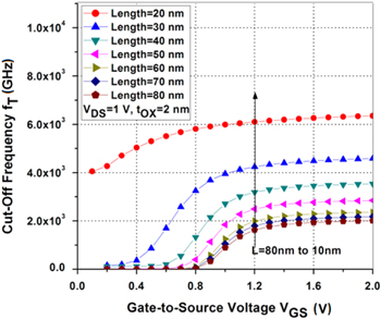
Figure 2. Unity-gain cut-off frequency (fT) as a function of gate-to-source voltage Vgs for different gate length.
Download figure:
Standard image High-resolution image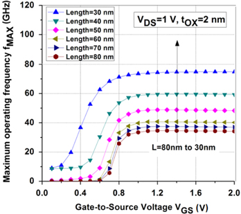
Figure 3. Maximum operating frequency fMAX as a function of gate-to-source voltage Vgs for different gate length.
Download figure:
Standard image High-resolution imageIt is evident from figures 2 and 3 that the unity-gain cut-off frequency fT and maximum operating frequency fMAX initially increase after VGS attain a specific value (threshold voltage). After the increase, they saturate at a higher Vgs. The initial increase of the fT and fMAX is driven by increasing on-current level due to the increasing gate bias, then it falls with gate bias due to the combined effect of the accelerated increase of the total gate-to-drain/source parasitic capacitances and the limite of gm due to mobility reduction by the gate field. The peak point of fT corresponds to the point between the minimum gate-drain/source capacitance and peak of gm. The value of fMAX is lower than fT due to the consideration of various parasitic components in the expression of fMAX. As the channel length decreases, the rate of fMAX increment is limited by the dominant effect of those increasing parasitic components.
3.2. Variation of radius R
Figure 4 shows the comparison between the trends related to the variation of unity-gain cut-off frequency fT along the downscaling of radius R. fT increases with reduction in R. It mainly attributes to the fact that, for a given gate length, it is expected that as the channel body gets wider, the gate electrostatic control on the channel regions gets weaker, lower gm can be achieved. Now overlap and fringing capacitances also increase and become dominant as radius R decreases.
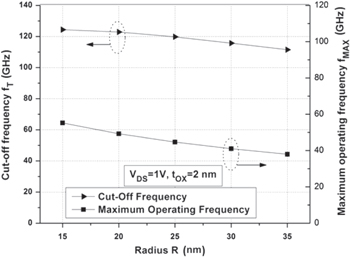
Figure 4. Unity-gain cut-off frequency (fT) and maximum operating frequency (fMAX) as a function of gate-to-source voltage (Vgs) for different values of radius R.
Download figure:
Standard image High-resolution imageTherefore, with downscaling of radius R, the Cgd/Cgs ratio is decreasing linearly. An increase in Cgd/Cgs ratio implies a loss of channel charge and the increase in parasitic feedback capacitance. Recently, underlap channel architecture has been employed to improve Cgd/Cgs ratio due to the enhanced gate controllability and less parasitic capacitance [18] it offers. It is evident that fMAX increases with the reduction in R, because smaller R leads to a) higher gate-controllability b) reduction in gds due to better suppression of drain terminal impact in thinner nanowire [19] and c) higher Cgd/Cgs ratio.
3.3. Variation of oxide thickness
As the thin body thickness is decreased, effective gate capacitance is increased and barrier height is decreased. However, electron mobility also reduces and results in a decrease in drain current (Id) and transconductance gm. Note that, since outer fringing capacitance Cof dose not change with thin body thickness, changes in fringing capacitance in this case are predominantly due to changes in inner fringing capacitance Cif.
Hence, as thin body thickness is reduced, total effective gate capacitance Cg eff is increased. To avoid mobility degradation and improve Ion, intrinsic silicon is used as the channel. To achieve good short-channel and RF performance, the only way is to reduce the oxide thickness tox according to equation (2). Figure 5 clearly shows that with reducing tox, device performance is greatly improved. Figure 2 also shows that RF performance improves considerably in both non-doped channel and heavily doped channel when the gate oxide thickness is reduced. The effects of tox on cause's threshold voltages shift towards lower values when tox increases.
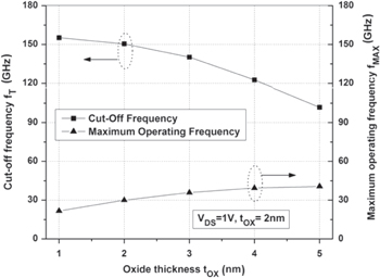
Figure 5. Unity-gain cut-off frequency (fT) and maximum operating frequency (fMAX) as a function of various oxide thickness tOX.
Download figure:
Standard image High-resolution image3.4. Variation of doping
With a decrease of source drain doping (undoped channel experiment), subthreshold swing, Ioff, and drain-induced-barrier-lowering (DIBL) are greatly improved. The only trade-off is Ion. There is no obvious trend in device performance improvement as channel doping is reduced. But it is found that DIBL and sub-threshold swing in undoped channel are slightly reduced as compared with heavily doped channel. There are two factors that dominate device performance as channel doping varies. One is flat-band shift due to channel doping—as channel doping drops, flat-band shifts negatively and leads to threshold voltage VTh drop and Ioff rise. With decreasing channel doping, depletion thickness rises and subthreshold performance is improved. Undoped channel is usually used in full-depleted silicon-on-insulator (SOI) devices to reduce surface scattering of carriers as the channel thickness is scaled down. With the source and the drain extension (SDE) doping gradient increasing, the outer fringing capacitance and overlap capacitance increase and ultimately lead to the increase of the total gate capacitances. With the increasing doping gradient, the resistance decreases dramatically. Due to the trade-off between the parasitic capacitances and resistance an optimization is required.
Figures 6 and 7 are unity-gain cut-off frequency (fT) and maximum operating frequency (fMAX), respectively, as functions of gate-to-source voltage for various doping concentrations.
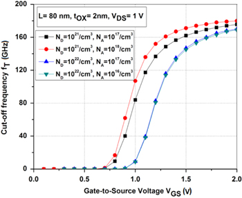
Figure 6. Unity-gain cut-off frequency (fT) as a function of gate-to-source voltage for various doping concentrations.
Download figure:
Standard image High-resolution image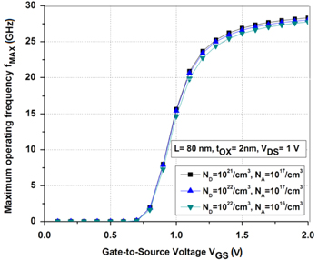
Figure 7. Maximum operating frequency (fMAX) as a function of gate-to-source voltage for various doping concentrations.
Download figure:
Standard image High-resolution image3.5. Variation of overlap/underlap
The total effective gate capacitance can be expressed [20] as Cg eff = series(COX, CSi) || COV || Cif || Cof, where COV depends on the overlap length, oxide thickness and channel width, CSi denotes capacitances offered by silicon, Cif denotes inner fringe capacitance and Cof denoted outer fringe capacitance. Oxide capacitance per unit area COX is a function of channel length L, channel width W and oxide thickness tox. Gate-to-source/drain overlap assures good electrostatic control of the channel, and hence, a strong ON-state current Ion, but excessive Miller capacitance degrades the switching performance.
On the other hand, while the parasitic overlap capacitance can be reduced in an underlapped device, the high series resistance causes a low current drive with reduced SCE. However, underlap on the source side leads to significant degradation in ON-current as well as increased effect of process variations on the threshold voltage. The results imply that gate-overlap architecture is preferred in SNWTs, which is quite different from the results of double-gate (DG) MOSFETs, where gate-underlap architecture is beneficial [16, 21, 22]. The effective gate capacitance initially increases with the increase in overlap and then becomes flat. Inner fringing capacitance Cif increases with overlap due to the decrease in distance between the source/drain with the gate. At strong inversion, however, Cif vanishes because the inversion layer screens the fringing field. This is because total gate capacitance Cg is dominated by the fringing capacitance (Cfr), which is a logarithmic function of the overlap [23, 24]. While Cg decreases with gate overlap, Ion and Ioff also increases with increasing overlap. This is primarily attributed to the fact that with the increase of gate overlap the effective channel length decreases, as a result drain current increases. Hence, for large enough overlap the current is inversely proportional to the channel length and increases linearly with the increase in overlap. For SNWTs, this is probably due to the following facts. First, the reduction of the parasitic resistance of the SDE regions appears to be very stringent for nanowire structure. Parasitic capacitances, however, are less sensitive to the doping gradient compared with DG MOSFETs, since the main contributor to the parasitic capacitance is the outer-fringing capacitance, as long as the doping profile is not too much of a gradient to induce considerable overlap capacitance. For DG MOSFETs, an important factor for the adoption of gate-underlap architecture is that it can offer good suppression of over SCE degradation. However, our simulation results reveal that gate-underlap architecture is not necessary for SNWTs from the perspective of SCE immunity because GAA structure has already ensured acceptable SCE effects.
Figures 8 and 9 are unity-gain cut-off frequency fT and maximum operating frequency fMAX, respectively, as functions of gate-to-source voltage for gate underlap and overlap.
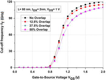
Figure 8. Unity-gain cut-off frequency fT as a function of gate-to-source voltage for gate underlap and overlap.
Download figure:
Standard image High-resolution image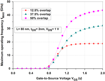
Figure 9. Maximum operating frequency fMAX as a function of gate-to-source voltage for gate underlap and overlap.
Download figure:
Standard image High-resolution image
4. Conclusion
In this paper the RF performance characteristics investigation of a surrounding gate MOSFET with varying parameters such as thickness of oxide tOX, channel length L, radius R of cylindrical surrounding gate MOSFET, doping concentrations Nd and Na, and the gate symmetry is presented. The various figure-of-merits of RF performance parameters are evaluated by 2D device simulator ATLAS from Silvaco.