
Abstract
In this paper we focus on silicon nanowires (Si-NWs) which were fabricated on transparent conductive substrates by plasma-enhanced chemical vapor deposition (PECVD) method using Sn as stimulated catalyst metal. Transparent conductive substrates which we used are ZnO fabricated by direct current (dc) sputtering. Property of ZnO thin film was investigated by x-ray diffraction (XRD), volt-ohm-miliampere (VOM) meter, and Stylus method. In order to grow Si-NWs using PECVD we need to use metal as catalyst. We used Sn as catalyst to synthesize Si-NWs. Sn catalyst nanoparticles were fabricated by high vacuum evaporation system (SenVact). Size and density of Sn catalyst nanoparticles were investigated by scanning electron microscope (SEM). The influence of the thickness of metal layers on forming Sn catalyst nanoparticles was studied. In particular, the factors affecting the formation of Si-NWs such as temperature and rate of gas were examined. Si-NWs' properties were investigated by SEM, Raman spectroscopy and energy dispersive x-ray (EDX) spectrocopy.
Export citation and abstract BibTeX RIS

Original content from this work may be used under the terms of the Creative Commons Attribution 3.0 licence. Any further distribution of this work must maintain attribution to the author(s) and the title of the work, journal citation and DOI.
1. Introduction
Silicon nanowires (Si-NWs) have many unique properties which are a perspective for further applications in the production of optoelectronic devices such as sensors, solar cells, transistors and so on [1, 2]. Although they were synthesized by many methods and some of them give satisfactory results, their application for photovoltaic devices are still ineffective. So we need to improve not only deposition process, optical and electrical quality of nanowires, but also the final incorporation into multi structure of nanowires. Si-NWs can perform with different catalyst metals such as Au, Al, Sn, Ti [3]. Among those metals, Sn has many positive properties. Sn has a low eutectic point (232 °C), so Si-NWs synthesis process was carried out more easily. Furthermore, Sn does not have deep impurity level in the band gap of Si, so it does not affect lifetime of carriers. Otherwise, Sn is removed easily after Si-NWs synthesis through the reaction Sn + H2 → SnHx [2]. However, using Sn as catalyst for Si-NWs synthesis faces some challenges. Sn does not like Au, which has two electrons on the outer player, Sn has four electrons on the outer player, so it cannot interact with SiH4 gas molecules from the environment to decompose the Si-H associate that is a prerequisite for Si-NWs synthesis.
Tin-catalyzed silicon nanowires have been synthesized by Rathi [4] and Jeon [5]. But all were integrated on substrates such as silicon wafers, corning or glass. For the purpose of using Si-NWs for optoelectronic devices, we need to synthesize Si-NWs on transparent conductive thin film (ZnO). So in our study, we synthesize Si-NWs on transparent conductive ZnO substrates using Sn as stimulated catalyst metal; then we investigate influences of ZnO substrates on the structure and orientation of the Si-NWs.
2. Experimental
First corning substrate surface of the size 5 × 10 mm2 is treated with a solution of 10% HF for 5 s. Next it is rinsed with deionized water in ultrasonic for 2 min, then dried by centrifugation machine. Finally, it is put into the vacuum chamber of an unbalanced dc magnetron sputtering system to fabricate ZnO transparent conductive thin film.
The experiment of the ZnO deposition process was carried out according to the diagram shown in figure 1 with corning substrates placed perpendicular to the target to prevent negative ion flow going backward to bombard the substrate [6]. Fabrication parameters are shown in table 1.
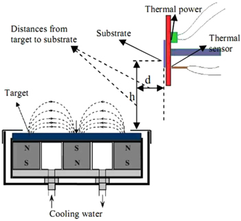
Figure 1. Schematic diagram of dc magnetron sputters for ZnO thin films.
Download figure:
Standard image High-resolution imageTable 1. Sputtering conditions of ZnO thin films.
| Temperature of substrate | Horizontal distance | Vertical distance | Pressure of argon | Voltage | Current | Time of deposition | Target |
|---|---|---|---|---|---|---|---|
| 200 °C | 25 mm | 40 mm | 0.4 Pa | 500 V | 200 mA | 30 min | ZnO |
For deposition of catalyst Sn layer we use the SenVact thermal evaporation system. Sn was evaporated and deposited with various thicknesses to study the formation of Sn metal nanoparticles table 2. After fabricating Sn catalyst nanoparticles we used PECVD system to study the effects of environmental temperature and plasma on Sn catalyst nanoparticles. The survey parameters are shown in table 3. Si-NWs were fabricated by PECVD system with experience conditions shown in table 4.
Table 2. The evaporation conditions of Sn layers.
| Pressure | Substrate's temperature | Thicknesses | Rate of evaporation | Specific mass | Boat | Material |
|---|---|---|---|---|---|---|
| 1.4 × 10⁻³ Pa | Room temperature | 5 nm, 10 nm, 100 nm |
|
0.724 g cm−3 | Tungsten | Sn |
Table 3. Affecting survey conditions of temperature and plasma on Sn catalyst nanoparticles.
| Frequency | Temperature | Time | Hydrogen flow | Sn thickness | Pressure |
|---|---|---|---|---|---|
| 13.56 MHz | 250 °C, 350 °C, 450 °C | 5 min | 50 sccm | 5 nm | 77 Pa |
Table 4. Si-NWs fabrication conditions in PECVD system.
| Substrate | Temperature | Pressure | Power of plasma | Catalyst metal | RF frequency | Time of deposition | H2/SiH4 rate |
|---|---|---|---|---|---|---|---|
| ZnO | 200 °C, 250 °C, 350 °C, 450 °C | 77 Pa | 10 W | Sn (5 nm) | 13.56 MHz | 20 min | 10:1, 20:1, 30:1, 35:1, 40:1 |
The properties of ZnO were investigated as thickness was determined by the stylus method, the conductivity and transmittance are determined by four-point probe method and UV–Vis spectrum, the structure was determined by XRD. ZnO surface morphology, Sn catalytic nanoparticles, and Si-NWs were determined by SEM. The Si-NWs' structure was determined by Raman spectroscopy method. EDX spectrum was used to determine the catalyst nanoparticles on Si-NWs top.
3. Results and discussion
3.1. Fabricating ZnO transparent conductive thin film
ZnO transparent conducting films that were fabricated by dc magnetron have good optoelectronic properties: the conductivity of about 1.2 × 10⁻³–2.1 × 10⁻³ Ω cm is shown in table 5; transmittance higher than 80%, uniform surface morphology, structure and development orientation of (002) network face are shown in figure 2.
Table 5. Conductivity of nine random ZnO thin film samples.
| Samples | Thickness (nm) | Face resistivity (Ω) | Resistivity (10−3 Ω cm) |
|---|---|---|---|
| 1 | 1125 | 18 | 2.03 |
| 2 | 1000 | 18 | 1.80 |
| 3 | 750 | 25 | 1.88 |
| 4 | 760 | 21 | 1.52 |
| 5 | 1100 | 17 | 1.87 |
| 6 | 1150 | 18 | 2.07 |
| 7 | 1150 | 19 | 2.18 |
| 8 | 750 | 17 | 1.20 |
| 9 | 830 | 19 | 1.16 |
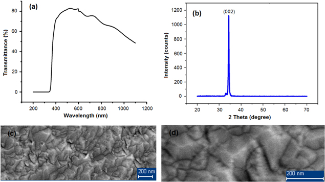
Figure 2. (a) UV–Vis spectrum, (b) XRD spectrum and SEM pictures of surface morphology at (c) 20 000, (d) 50 000 times.
Download figure:
Standard image High-resolution image3.2. Fabricating Sn catalyst nanoparticles
When metal thin films were deposited on solid substrates, they will trend toward self-forming metal droplet which has least energy and is most durable [7]. Figure 3 shows the catalytic Sn nanoparticles with different thicknesses coated with a transparent conductive film.
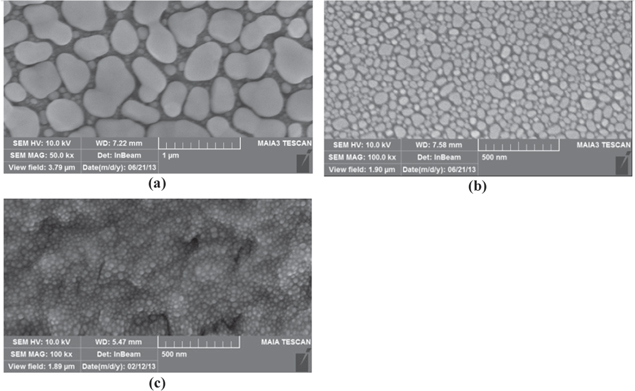
Figure 3. SEM images of Sn catalyst nanoparticles formed on ZnO with different thickness (a) 100 nm, (b) 10 nm and (c) 5 nm.
Download figure:
Standard image High-resolution imageDifferent thicknesses of the metal thin film lead to different sizes of Sn catalyst nanoparticles. The average size of Sn nanoparticles increases if thickness of deposited Sn layer increases. The average radii of Sn catalyst nanoparticles are 20 nm, 28 nm and 105 nm corresponding to metal thicknesses of 5 nm, 10 nm and 100 nm. This occurs because large Sn nanoparticles swallow smaller Sn nanoparticles to form Sn nanoparticles with larger size.
During Si-NWs synthesis process using PECVD there are some aspects affecting Sn catalyst nanopaticles such as temperature, plasma and hydro environment. Results have shown that plasma in hydro environment affects the density of Sn nanoparticles. This is shown in figure 4.
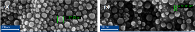
Figure 4. SEM images of nanoparticles at (a) before and (b) after Sn nanoparticles annealing in a hydro environment with plasma.
Download figure:
Standard image High-resolution imageObservation of SEM and the statistic process showed that Sn diameters have not changed, but the density of Sn nanoparticles has changed. Observation of the same sample was done after and before Sn nanoparticles annealing in plasma and hydro environment. There are about 1639 Sn pieces/μm2 before annealing and 1055 Sn pieces/μm2 after annealing (decrease of about 30% in quantity). Density reduction phenomenon occurs due to corrosion of Sn in H2 environment through a stimulating effect of plasma leading to a chemical reaction to form SnHx gaseous products. This has also been mentioned in the study of Somikumar [4].
3.3. Synthesized Si-NWs
3.3.1. Si-NWs synthesized by vapor liquid solid mechanism
Growth of Si-NWs following vapor liquid solid (VLS) mechanism must have three aspects, namely (i) synthesized temperature is the higher eutectic point, (ii) there are catalyst metal nanoparticles and (iii) catalyst metal nanoparticles have been observed on the head of Si-NWs after the synthesis process. Figure 5 shows these three aspects.

Figure 5. (a) SEM image of sample synthesized at lower eutectic point, (b) SEM image of sample which has half the side with Sn catalyst and the remaining side without Sn catalyst, (c) SEM image confirms the existence of Sn nanoparticles on the head of Si-NWs, (d) map data on EDX spectrum confirms Sn nanoparticles.
Download figure:
Standard image High-resolution imageThe Si-NWs only appear in the places where the temperature is higher than eutectic point and there are catalytic metal nanoparticles [7]. The Si-NWs growth process through VLS mechanism has gradually raised catalytic metals up and we can observe catalyst metals on the head of Si-NWs. Map data of the EDX spectrum have shown that green points which appear on the heads of Si-NWs are Sn catalysts.
3.3.2. Si-NWs synthesized with different temperatures
One of the aspects affecting Si-NWs growth is the temperature of the substrate in Si-NWs synthesis process. This was observed clearly in figure 6.
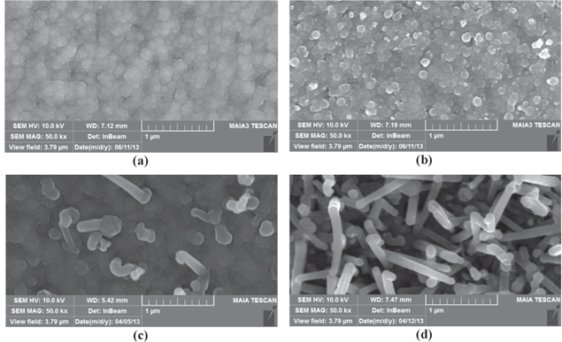
Figure 6. SEM images of Si-NWs synthesized at different temperatures (a) 200 °C, (b) 250 °C, (c) 350 °C, (d) 450 °C.
Download figure:
Standard image High-resolution imageIn the sample synthesized with 200 °C substrate there no Si-NWs appeared on the surface. This can be explained as follows: Si-Sn two-component liquid alloy has not been created so Si-NWs have not grown through VLS mechanism. When temperature increases to the 250 °C higher eutectic point, liquid two-component alloy has been created and observed by SEM as white points. But the substrate's temperature higher eutectic point still does not ensure Si-NWs growth, which depends on some different conditions. Si-NWs only appear clearly when the substrate's temperature is 350 °C or higher. The higher the substrate's temperature, the faster the speed of Si-NWs deposition and growth, leading to density and length of Si-NWs increasing. Samples have been synthesized with the substrate's temperature lower than 350 °C and there are only amorphous silicon layers coated onto the surface of the sample. This was verified through Raman spectra of figure 7.

Figure 7. Raman spectrum of Si-NWs synthesized at different temperatures.
Download figure:
Standard image High-resolution imageThe Si-NWs synthesized with the substrate's temperature at 200 °C and 250 °C are amorphous with broad spectral peak located at about 480 cm−1. When the substrate's temperature increases up to 350 °C and 450 °C, peaks at 520 cm−1 position have appeared, proving that crystal Si has been formed. This can be explained as follows: with increasing temperature the energy supply leads to the rearrangement of Si atoms to form local crystalline structures which are micro or nano-crystals. That has been confirmed through the shape of peaks at 520 cm−1 position which are wider than the peak of crystalline Si. Peak of the sample at 450 °C is higher than the sample at 350 °C, proving that crystalline density of the sample at 450 °C is higher than that of the sample at 350 °C.
3.3.3. Si-NWs synthesized with different gas rate of H2/SiH4
Changing H2/SiH4 affects the growth of Si-NWs and leads to affecting structure, density, size and shape of the Si-NWs. This is shown very clearly in figure 8.

Figure 8. SEM pictures of Si-NWs synthesized at different H2/SiH4 gas rates (a) 10:1, (b) 20:1, (c) 30:1, (d) 35:1, (e) 40:1 and (f) statistics of the density.
Download figure:
Standard image High-resolution imageAt first, when the rate of H2 in the H2/SiH4 mixture increases, the density of Si-NWs reaches the highest value at 30:1 ratio. But if the rate of H2 still increases, the density of Si-NWs decreases and finally Si-NWs disappear at a 40:1 ratio. Changing density of Si-NWs is caused by two reasons. The first reason involves nanoparticles size of catalytic Sn. They are placed in an environment with SiH4 gas and plasma that causes them to be reconfigured, rearranged and to form a catalyst particle with larger size leading to density of catalyst nanoparticles reducing [5]. The second reason involves the incubation period of catalyst nanoparticle seeds. The incubation period is the time for the catalytic nanoparticles to get enough Si atoms to achieve super-saturation state [8]. So there is too much H2 in H2/SiH4 mixture; catalyst nanoparticles cannot achieve super-saturation state so that Si-NWs have not grown. Furthermore, at the same time the a-Si:H layer deposition process also takes place and it could bury catalyst nanoparticles that make catalyst nanoparticles fail to reach the supersaturation state to develop Si-NWs.
Development orientation of Si-NWs is the direction [202], [0–22] with angle about 45° and direction [−111], [111] with angle about 100°. This is observed in figure 9. The structure of the Si-NWs analyzed via Raman spectrum is shown in figure 10.
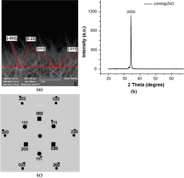
Figure 9. (a) SEM image shows the development of the orientation of Si-NWs, (b) XRD spectrum of ZnO substrate, (c) development of the orientation in XRD spectrum.
Download figure:
Standard image High-resolution image
Figure 10. Raman spectrum of Si-NWs synthesized at different H2/SiH4 gas ratios.
Download figure:
Standard image High-resolution image
At the largest H2/SiH4 ratio (1:10), a peak only appears at 480 cm−1 and it has a wide radius, showing that Si-NWs are amorphous silicon. The main reason for the formation of amorphous structure depends on speed of Si-NWs growth. Large SiH4 ratio makes a fast Si deposition rate; the re-configuration process of Si to form crystalline structure is very hard. When SiH4 ratio in mixture H2/SiH4 decreases, crystalline structure also increases considerably. That is expressed through a spectral peak at 520 cm−1 position while the characteristic peak of amorphous silicon at 480 cm−1 appears with very low intensity. All are explained by the synthesis process, Si-NWs are supplied at high temperature (450 °C) and deposited Si atoms have more mobility. They rearrange and restructure to form the local crystal. There is a little peak shift at 1:30 and 1:40 gas ratio compared with standard 520 cm−1 peak of single-crystal Si. This shift is caused by the structure of the samples which are mixture structures of amorphous components and nano-crystalline intermediates [9].
4. Conclusion
From the results of this research we can conclude that Si-NWs has been successfully synthesized by PECVD system on conductive transparent ZnO thin film, which opens a wide potential to use Si-NWs.
We have also successfully fabricated transparent conductive ZnO thin films by dc magnetron sputtering with good results such as transparency of film being about 80%, the resistivity of film can reach 1.52 × 10⁻³ Ωcm and the surface is quite smooth.
We have investigated factors which affect the development of the Si-NWs on ZnO thin film such as temperature, gas ratio and metallic Sn nanoparticles. We have determined that Si-NWs synthesized at 450 °C and with a H2/SiH4 gas ratio of 20:1 have good quality: wire diameter is about 100 nm, wire length is about 1.5–2 μm, growth directions are, [202], [0–22], [−111], [111].