Abstract
In this paper, the existing two-dimensional (2D) threshold voltage model for a dual material gate fully depleted strained silicon on insulator (DMG-FD-S-SOI) metal-oxide-semiconductor field effect transistor (MOSFET) is modified by considering the interface trapped charge effects. The interface trapped charge is a common phenomenon, and this charge cannot be neglected in nanoscale devices. For finding out the surface potential, parabolic approximation has been utilized and the virtual cathode potential method is used to formulate the threshold voltage. The developed threshold voltage model incorporates both positive as well as negative interface charges. Finally, validity of the presented model is verified with 2D device simulator Sentaurus™.
Export citation and abstract BibTeX RIS

Original content from this work may be used under the terms of the Creative Commons Attribution 3.0 licence. Any further distribution of this work must maintain attribution to the author(s) and the title of the work, journal citation and DOI.
1. Introduction
The feature sizes of metal-oxide-semiconductor field effect transistors (MOSFETs) are being continuously decreased to increase the packing density, as very large scale integration technology advances. However, the short channel effects (SCEs) are posing serious threats for further scaling to follow the ITRS roadmap [1]. For a bulk MOSFET, continuous scaling requires increasing the channel doping to achieve a lower junction electric field in the channel. Also, the higher doping ensures the non-overlap of the source and drain depletion widths in the channel region. However, a serious amount of mobility degradation occurs because of impurity scattering in the high channel doping region [2]. To encounter this problem, various new structures with different engineering concepts have been reported to reduce the SCEs in SOI platform. Among them, strain engineering is very popular for enhancing the carrier mobility [3, 4]. Strained Si provides device performance enhancements through changes in material properties rather than changing device geometry and doping.
The conventional method of producing strained-Si is growing pseudomorphic Si epitaxial layer on relaxed SiGe alloys. By increasing the Ge content of the relaxed SiGe alloy, the amount of biaxial strain, and therefore, the magnitude of the mobility is enhanced [5–8]. However, as the Ge content is increased, the critical thickness (the thickness to which the strained-silicon can be grown without inducing misfit dislocations to alleviate the strain) is reduced. Single layer strained-silicon-on-insulator (S-SOI) is a new SiGe-free material system that combines the carrier transport advantages of strained-Si with the reduced parasitic capacitance and improved MOSFET scalability of thin-film SOI MOSFET. The single layer S-SOI is less susceptible to misfit dislocation induced leakage current while maintaining increased carrier mobility [9–11].
For the first time, Kumar et al [9] proposed a simple analytical model of threshold voltage for single layer FD-S-SOI MOSFET in 2006. They had shown the dependency of various parameters such as Ge mole fraction (X), strained silicon thickness (tSi) and doping concentration on the threshold voltage. Jin et al [12] proposed a two-dimensional (2D) threshold voltage model for DMG strained SOI MOSFET. They have discussed how effectively the device was able to supress the hot carrier effects (HCEs) and threshold voltage roll-off. Similarly, the effect of double layer strain (i.e. strained silicon on SiGe relaxed layer) has been discussed by Bhusan et al [2]. They have also discussed the improved SCEs because of the DMG and strain silicon. However, nobody has considered the effect of interface trap charges while solving the 2D Poisson's equation.
In this work, the previously existing analytical model for surface potential, electric field, and threshold voltage for a dual material gate fully depleted strained silicon on insulator (DMG-FD-S-SOI) is modified with including the effects of interface charges. The interface charges are considered both in magnitude and polarity with an assumption that the charge distribution is uniform along the channel. Parabolic approximation method is used for solving the 2D Poisson's equation to formulate the surface potential and further virtual cathode potential method is used for modeling the threshold voltage which is elaborated in appendices
Along with the introduction, section 2 describes the device structure description that includes all the dimensions, materials and doping concentrations of DMG-FD-S-SOI MOSFET. This section also analyses the physics of the device using device numerical simulations and models activated for simulation. Section 3 comprises the modeling of surface potential, electric field, and threshold voltage. The impact of numerous device parameters on the surface potential, electric field, and threshold voltage of the DMG-FD-S-SOI MOSFET is discussed in section 4. Finally, the concluding remarks in section 5 substantiate the novelty of the paper.
2. Device structure
The schematic diagram of the DMG-FD-S-SOI MOSFET structure used for modeling and simulation is shown in figure 1. The device has uniformly doped source–drain with doping concentration of ND = 1 × 1020 cm−3. The channel is kept lightly doped with doping concentration of NA = 1 × 1016 cm−3. The gate oxide thickness, buried oxide thickness and the silicon are tox = 2 nm, tb = 50 nm and ts-Si = 10 nm, respectively. The damaged region due to the interface oxide trap charges (NF) is shown as a black line towards the drain side.
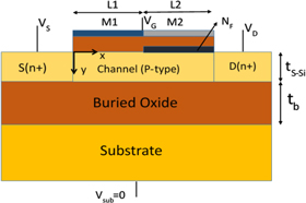
Figure1. Schematic structure of dual material gate fully depleted strained silicon on insulator MOSFET.
Download figure:
Standard image High-resolution imageThe gate length is divided into two parts as L1 and L2 for the use of two different gate electrodes. The work function of the gate material is: ϕM1 = 4.8 eV (e.g., Cu) and ϕM2 = 4.6 eV (e.g., Mo). The simulation is carried out by the device simulator Sentaurus, a 2D numerical simulator from Synopsis [13]. To study the surface potential along the channel we have taken the cutline at the surface of the channel thickness across the channel of the device. To obtain accurate results for MOSFET simulation we need to account for the mobility degradation that occurs inside inversion layers. The drift-diffusion model in default of carrier transport model in Sentaurus device is activated. The basic mobility model is used, which takes into account the effect of doping dependence, high-field saturation (velocity saturation), and transverse field dependence. The impact ionization effects are ignored. The silicon band gap narrowing model that determines the intrinsic carrier concentration is activated. The solution of the device equations are done self-consistently, on the discrete mesh, in an iterative fashion. For each iteration, an error is calculated and the device attempts to converge on a solution that has an acceptably small error. The Poisson equation, continuity equations, and the different thermal and energy equations are included in simulation [13]. All the structure junctions assumed as abrupt, and the biasing conditions considered at room temperature in the simulation.
3. Analytical model formulation
3.1. Surface potential formulation
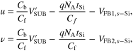
The modeling of surface potential for DMG-FD-S-SOI MOSFET is adopted from Jin et al [12], however we have considered trap charge effects/damaged region near the drain side by modifying the flat band voltage at drain side as
where  ,
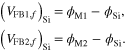
,  is the flat band voltage of strained-Si MOSFET in the front channel under M2 region.
  is the flat band voltage of bulk Si MOSFET in the front channel for M2 region.
  represents the amount of change in flat band voltage due to strain.
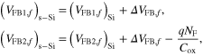
  is the interface oxide charges in both dimension and polarity and
  is the gate capacitance.
By considering  , we have remodeled the existing surface potential, electric field and threshold voltage model [9, 12, 14] to know the effect of interface trapped charges on various performance parameters of DMG-FD-S-SOI MOSFET. Finally solving the Poisson's equation using the predefined boundary conditions with a little modification of flat band voltage near the drain side, we obtained the surface potential as below [12]

The detailed mathematical conditioning and solution of  and
and  are given in appendix
3.2. Electric field formulation
Electric field horizontal component under metal gates M1/M2 can be calculated by differentiating the potential with respect to x:


The minimum potential of front channel can be expressed as


3.3. Threshold voltage formulation

A generalized evaluation method of Vth is presented in appendix
4. Results and discussion
In this section, results obtained from theoretical models of the surface potential, electric field and threshold voltage are compared with the numerical simulation results for DMG-FD-S-SOI MOSFET. Figure 2(a) demonstrates the surface potential curve along the channel length at various values of the drain voltage. Because of the presence of dual metal, the variation of channel potential under metal gate 1 (M1) with respect to drain voltage is quite small. The drain voltage is not absorbed under M1 as it is absorbed by metal gate 2 (M2), hence the channel under M1 is screened from the changes of drain potential. As a consequence, VDS has only a small influence on drain current after saturation. Also, due to the dual metal gate, the variation of channel potential minima with respect to drain voltage is quite small which minimizes the drain induced barrier lowering (DIBL) effect. In figure 2(b), the calculated and simulated values of surface potential are plotted against the horizontal distance x for L = 100 nm (L1/L2 = 1:1) at different values of effective Ge mole fraction (X) in the relaxed SiGe buffer. It can be seen that the potential barrier height is decreasing with increase in X. As the threshold voltage is calculated from the minimum surface potential, it is very important to choose the appropriate value of threshold voltage for the device. The device having high threshold voltage is slower. Similarly, the device having low threshold voltage has more leakage current. So, for our convenience, from figure 2(b), the middle one is considered, i.e., X = 0.2 and the value is fixed to study the effect of other parameters on surface potential for a DMG-FD-S-SOI MOSFET.

Figure 2. Variation of surface potential along the channel length, (a) for various drain voltages, (b) for different Ge mole fraction (X). Parameters used ϕM1 = 4.8 eV, ϕM2 = 4.6 eV, NA = 1 × 1016 cm−3, tSi = 10 nm, L = 100 nm, tox = 2 nm, and VGS = 0.1 V.
Download figure:
Standard image High-resolution imageFigures 3(a) and (b) depict the surface potential with the metal gate length ratio variations for positive charges and negative charges in the oxide interface, respectively. As seen from the figure, the increase in the length of metal gate nearer to drain, i.e. M2, raises the minimum surface potential and shifts it towards the source side. The position of the minimum surface potential is closer to source for a greater length of M2 region than lesser M2 length. This indicates a higher SCE in the device as the M2 extends more. This will further lower the source channel barrier height and hence a higher threshold voltage roll-off. However in the case of negative interface charges, the increase of the length of M2 region decreases the minimum surface potential. This will give a higher source-channel barrier height and hence a lower threshold voltage roll-off. The shifting of the minimum surface potentials is opposite to that in the positive interface charge case i.e. the minimum surface potential point shifts towards drain side as M2 length increases.
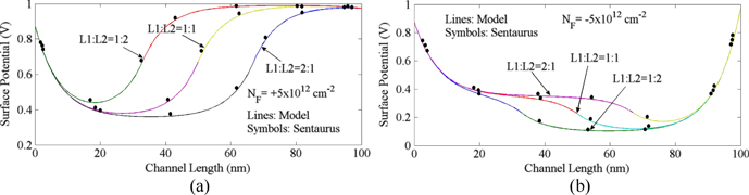
Figure 3. Variation of surface potential along the channel length for different gate length ratios (L1/L2 = 1:2, 1:1, 2:1) considering (a) positive interface charge, (b) negative interface charge. Parameters used X = 0.2, NF = +5 × 1012 cm−2, NF = −5 × 1012 cm−2, ϕM1 = 4.8 eV, ϕM2 = 4.6 eV, NA = 1 × 1016 cm−3, tSi = 10 nm, L = 100 nm, tox = 2 nm, VDS = 0.1 V and VGS = 0.1 V.
Download figure:
Standard image High-resolution imageFigure 4 shows the surface potential variation along the channel length for different amounts and polarities of interface trapped charges in the oxide. From the figure, the minimum of the surface potential is at the channel center for the device having NF = 0 and is moving towards the source and drain side, for positive and negative interface charge cases respectively. A positive interface charge case will obligate higher SCE on the device than its negative charge counterparts due to lower barrier height. However, the device having negative interface charges will cause more DIBL effect as the minimum potential point shifts towards the drain side. So both positive and negative interface charges are undesirable for the device performance.
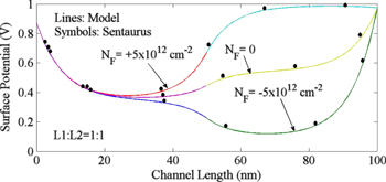
Figure 4. Surface potential variation along the channel length for interface charge variations (in magnitude and polarity). Parameters used X = 0.2, ϕM1 = 4.8 eV, ϕM2 = 4.6 eV, NA = 1 × 1016 cm−3, tSi = 10 nm, L = 100 nm, tox = 2 nm, VDS = 0.1 V and VGS = 0.1 V.
Download figure:
Standard image High-resolution imagefigure 5(a) shows the variation of the electric field distribution along the channel at different values of effective Ge mole fraction (X). It is evident from the figure that the electric field at the drain side considerably reduces with increase in X value. This reduction of the electric field experienced by the carriers in the channel can be interpreted as the reduction of the HCE at the drain end. Figure 5(b) shows the variation of the electric field distribution along the channel for different amounts and polarity of interface trapped charges in the oxide. From the figure, the peak of the electric field lies at the interface of the two metal gates. The device having positive interface charge will give maximum electric field peak as compared to NF = 0 and NF negative cases. So, positive interface charge case will obligate higher SCE on the device than its negative charge counterparts due to high electric field.

Figure 5. Variation of electric field along the channel length (a) for different Ge mole fraction (X), (b) for interface charge variations (in magnitude and polarity). Parameters used ϕM1 = 4.8 eV, ϕM2 = 4.6 eV, NA = 1 × 1016 cm−3, tSi = 10 nm, L = 100 nm, tox = 2 nm, VDS = 0.1 V and VGS = 0.1 V.
Download figure:
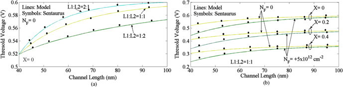
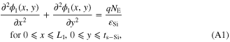
Standard image High-resolution imageFigure 6(a) shows the variation of threshold voltage with the channel length for different gate length ratios (L1/L2 = 1:2, 1:1, 2:1). It is observed that SCE become serious on decreasing the channel length ratios. That means the threshold voltage is higher for the higher control gate length i.e., length of M1. This is because of the higher channel barrier height for higher gate length ratio (L1/L2 = 2:1). This is attributed to the fact that the control gate (M1) loses its control over the channel at smaller length ratios. Figure 6(b) shows the threshold voltage variation along the channel length for NF = 0, negative and positive in the oxide. From the figure, the threshold voltage is higher in case of NF = 0 and it is lower for positive interface charge case. This is due to the lower barrier height in the case of positive interface charge. So, the device having interface trap charges is more prone to SCEs. The threshold voltage variation against channel length for different Ge mole fractions (X) can also be seen from the same figure. It is observed that the threshold voltage is higher for the NF = 0 case. Further, the variation of threshold voltage with gate length for different values of effective Ge mole fraction in the relaxed SiGe buffer is also shown in the same figure. It is observed that SCEs become apparent when the channel length is below 40–50 nm and is marked by sharp decrease in the Vth value. The gate-source/drain (S/D) charge sharing and source-body/drain-body built in potential barrier lowering due to overlap of the lateral source-body and drain-body depletion regions becomes significant for such short channel lengths. The Vth values from the analytical model are in close proximity with the simulation results.
Figure 6. Threshold voltage variation along the channel length (a) for different gate length ratios (L1/L2 = 1:2, 1:1, 2:1), (b) with interface charge variations (in magnitude and polarity) for different Ge mole fraction (X). Parameters used X = 0.2, ϕM1 = 4.8 eV, ϕM2 = 4.6 eV, NA = 1 × 1016 cm−3, tSi = 10 nm, L = 100 nm, tox = 2 nm, VDS = 0.1 V and VGS = 0.1 V.
Download figure:
Standard image High-resolution image
5. Conclusion
The modified model including interface trapped charges for surface potential, electric field and threshold voltage analyses the effectiveness of DMG-FD-S-SOI MOSFET to suppress the SCEs. Due to the dual material gate introduction, there is a step function in the channel region and that will be the important factor for suppression of HCE and DIBL. An extensive analysis is carried out to study the effect of various parameters such as Ge mole fraction, drain bias, gate length ratio variation, and interface charge variation on surface potential, electric field, and threshold voltage. From the result, the deterioration in the threshold voltage with increasing strain may be improved by increasing the length of control gate (M1). Also, by increasing the gate length ratio (L1/L2), DIBL and HCE can be controlled effectively. The device performance is going to deteriorate in the presence of the interface trapped charges in the oxide. The derived analytical model is compared and found to be in excellent agreement with the simulation results obtained from Sentaurus™.
Appendix A
The common Poisson's equation for the potential distribution in the two strained silicon regions can be written as [12]
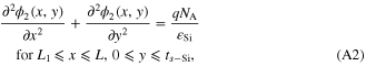
where  is the permittivity of strained Si film, NA is the doping concentration of strained Si film, and ts−Si is the thickness of strained Si film. The potential distributions in both two regions can be approximated by parabolic polynomial as [2]
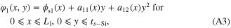
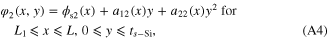
where ϕs1(x) and ϕs2(x) are the surface potential under gate electrodes M1 and M2, respectively. The coefficients of a11(x), a12(x), a12(x), and a22(x) are the functions of x only. The Poisson's equation can be solved by using the following boundary conditions.
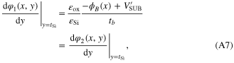
- (1) Electric flux (displacement) at the gate oxide/strained Si film interface is continuous in both regions:
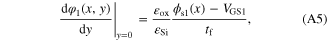
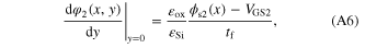
where 
 with
with  ox and tf are the permittivity of SiO2 and thickness of gate oxide. The effects of trapped charges are to be considered as:
The effect of strain on band structure is considered as given in [9], where  and
and  are the flat band voltages of strained-Si MOSFET in the front channel for both the regions.
  and
and  are the flat band voltages of bulk Si MOSFET in the front channel for both the regions.
  represents the amount of change in flat band voltage due to strain.
  is the interface oxide charges in both dimension and polarity and
  is the gate capacitance.
- (2) Electric field at the interface of the buried oxide and the back channel is continuous
where 
 is the substrate bias,
  is the flat band voltage of strained silicon in the back channel and ϕB(x) is the back potential.
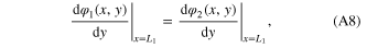
- (3) Electric flux (displacement) and the electric potential at the M1/M2 interface is continuous

- (4) The surface potential at the source end is

where  is the built-in potential of strained Si thin film [12].
- (5) The surface potential at the drain end is

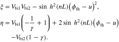
Using the boundary conditions equations (A5)–(A11) we obtain coefficients and obtain the expressions for ϕ1(x, y) and ϕ2(x, y). Substituting ϕ1(x, y) and ϕ2(x, y) into (A1) and (A2), respectively, and substituting y = 0, we obtain


where 


The solution for (A12) and (A13) as second order non-homogenous differential equations with constant coefficients can be expressed as
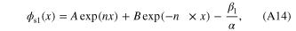
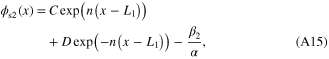
where 
 and
and 
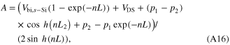
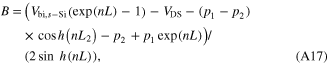
Using the boundary condition (A5)–(A11) we solve for A, B, C, and D


Appendix B
The minimum potential of channel can be calculated from (A14), (A15) as


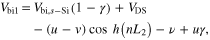
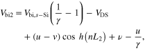
The threshold voltage (Vth) of the un-strained device can be found as follows [15]

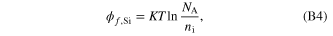
where K is the Boltzmann's constant, T is the temperature,  is the difference between the Fermi potential and the intrinsic Fermi is level in the bulk region, ϕth is the value of surface potential at which the volumetric inversion electron charge density in the Si device is equal to the body doping.
For strained-Si SOI MOSFET the threshold condition under the front gate is modified as [2]

where 
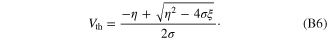
In the case of the DMG-FD-S-SOI structure, because of coexistence of different metal M1 and M2, the minimum surface potential is purely dependent on metal gate with the higher work function. So the threshold voltage is calculated as the value of VGS at which the minimum surface potential  equals to ϕth. Hence, one can determine the value of threshold voltage as the value of VGS by using formula (8)
where