

Abstract
Germanium (Ge) is a group-IV indirect band gap semiconductor but the difference between its direct and indirect band gap is only 140 meV. It has been shown that when Ge is subjected to a tensile strain and a heavy n-doping level, room-temperature photoluminescence (PL) can be greatly enhanced. Among these two factors, achieving a heavy n-doping level in Ge (i.e., electron concentrations higher than 1 × 1019 cm−3) is a challenge since the solubility of most group-V elements (P, As, Sb) in Ge is very low. We report here Ge growth on silicon substrates using molecular beam epitaxial (MBE) technique. To enhance the n-doping level in Ge, a specific n-doping process based on the decomposition of the GaP compound has been implemented. The GaP decomposition allows producing P2 molecules, which have a higher sticking coefficient than that of P4 molecules. We show that phosphorus doping at low substrate temperatures followed by flash thermal annealing are essential to get a high doping level. We have obtained an activate phosphorus concentration up to 2 × 1019 cm−3 and room-temperature PL measurements reveal an intensity enhancement up to 50 times. This result opens a new route for the realization of group-IV semiconductor optoelectronic devices.
Export citation and abstract BibTeX RIS

Original content from this work may be used under the terms of the Creative Commons Attribution 3.0 licence. Any further distribution of this work must maintain attribution to the author(s) and the title of the work, journal citation and DOI.
1. Introduction
In recent years, the synthesis of tensile-strained and heavily n-doped Ge thin films on Si has attracted growing interest due to the potentiality of using Ge as an active layer in optoelectronic devices that are fully compatible with the existing microelectronic Si technology [1–4]. It has been shown that when Ge is submitted to a tensile strain, its direct band gap can reduce faster than the indirect band gap and with a tensile strain of about 1.9%, Ge can become a direct band gap semiconductor [5]. However, it is difficult to get such a high value of strain in epitaxial Ge films. In practice, a tensile strain level of only about 0.2–0.3% was currently obtained in Ge films, grown either on Si or on III–V semiconductor substrates [6–8]. On the other hand, with application of ∼1.9% tensile strain, the Ge direct band gap can be reduced down to ∼0.5 eV and the corresponding wavelength of the emitted light shifts to 2500 nm, which is far from the wavelength range used in telecommunications.
Doping Ge with electrons can allow fulfilling the energy level in the indirect band gap. It has been suggested that when the n-doping concentration reaches a value as high as ∼7 × 1019 cm−3 [9], the electrons that are brought from n-doping will occupy the energy states in the indirect band gap up to a level, which is equivalent to the lowest energy level at the bottom of the direct band gap. Thus, Ge can become a pseudo direct band gap semiconductor and injected electrons that are brought from photoluminescence (PL) or electroluminescence experiments will have a much higher probability of occupying the direct Γ valley, thus highly efficient radiative recombinations will be expected. However, a high n-doping level in Ge remains a challenge to overcome. Compared to Si, the equilibrium solubility of group-V elements, such as P, Sb or As, is generally 3 to 5 times smaller in Ge [10], and consequently the highest n-doping level in Ge that has been commonly reported in the literature is in the range between 7 × 10¹⁸ and 1 × 1019 cm−3.
In this work we implement an alternative approach to realize a high n-doping level in Ge, which is based on the decomposition of the GaP compound to produce diphosphorus (P2) molecules that have a sticking coefficient of about 10 times larger than that of tetrahedral white phosphorus (P4) molecules [11, 12]. In general, an efficient doping process requires controlling two main parameters: the sticking coefficient of dopants on the film surface and the dopant solubility in the host matrix. Electrical and optical characterizations have been combined to study the effect of doping parameters, such as the temperature of the GaP cell, the substrate temperature and the annealing condition, in order to optimize the doping process. We show that the sticking coefficient of phosphorus on the growing film surface is the key parameter, allowing getting a high n-doping concentration. A doping process based on low-temperature doping, followed by flash thermal annealing has been established. It is shown that an active phosphorus concentration up to 2 × 1019 cm−3 can be achieved and PL measurements reveal an intensity enhancement up to 50 times.
2. Experimental details
Ge growth was carried out in a standard molecular beam epitaxial (MBE) system with a base pressure better than 3 × 10⁻¹⁰ mbar. The growth chamber is equipped with a 30 keV reflection high-energy electron diffraction (RHEED) apparatus, which allows us to monitor in situ and in real time the Ge growth mode. An Auger electron spectrometer is used to control the cleanliness of the substrate surface prior to growth and the efficiency of Ga trapping of the GaP source. Ge was evaporated from a two-zone heated Knudsen effusion cell and the Ge deposition rate, measured from RHEED intensity oscillations during Ge homoepitaxy on a Ge(111) substrate, was in the range between 1.5 and 5 nm min−1. The measured error of the Ge growth rate is less than 3%. More details of the experimental set-up and growth conditions can be found elsewhere [13].
The substrates were flat, p-type Si(001) wafers. Cleaning of the substrate surface was carried out using the hydrogen-terminated Si(001) method, which consists of two steps [14]: the first was a wet chemical treatment in NH4F solution to prepare an ideally SiH2-terminated Si(001) surface. The second step is heating the sample in ultrahigh vacuum to desorb the passivating hydrogen layer at a temperature below 500 °C. After this step, the Si surface exhibits a well-developed (2 × 1) reconstruction and AES measurements do not reveal any presence of oxygen or carbon.
The substrate temperature was measured using a thermocouple in contact with the backside of Si wafers. The accuracy of the temperature measurement is estimated to be about ±20 °C. The PL is measured with a 532 nm laser focused on the sample surface. The PL signal is measured with an InGaAs detector and the wavelength is cut off at 1600 nm. All PL spectra were recorded at room temperature. The film resistivity was measured at room temperature using a standard four-point probe technique. To insure the reproducibility of the resistivity measurement, gold (Au) contacts with a surface of about 3 mm2 were prepared on the top of the Ge surface using conventional optical lithography.
3. Results and discussion
It is well established that tetrahedral white phosphorus P4 molecules have a low sticking coefficient and different approaches have been proposed to improve the sticking coefficient of phosphorus molecules, in particular thermal molecular cracking cells. The decomposition of a P-based compound is an alternative approach and its operating principle is based on the decomposition of the GaP compound to provide high-purity P2 molecules and Ga atoms. At an intermediate temperature range, P2 molecules have a much higher vapor pressure than Ga, thus P2 molecules can easily escape from the cell while a great part of Ga atoms remains condensed at the bottom of the cell. To increase the efficiency of the P2 sublimation, a Ga-trapping cap system is placed on the top area of the cell. According to the cell supplier, the best P2/P4 ratio can reach a value up to 150:1 [15].
Therefore, one of our first objectives consists of determining the highest temperature range of the GaP cell at which the GaP decomposition can produce a high P2 flux while the Ga trapping cap remains efficient. Auger electron spectroscopy (AES) was used to evaluate the amount of Ga, which can escape from the cell and deposit on the sample surface. To do this, we expose a Ge surface in front of the GaP cell, heated at various temperatures, and record the evolution of the Auger Ge, P and Ge transitions. In order to have a sufficient resolution during AES analysis, the exposing time is about 30 min at each cell temperature. Figure 1 displays AES spectra measured at three different cell temperatures: 700, 750 and 800 °C. The bottom black curve corresponds to the AES spectrum of the initial Ge surface, where a main transition located at ∼47 eV is clearly observed (another Ge transition at 51 eV is less visible). After 30 min exposed to the GaP cell, the phosphorus transition located at 120 eV appears and its intensity increases with increasing the GaP cell temperature while Ga transitions at 55 eV are absent. This means that from AES measurements the Ga trapping appears efficient up to a cell temperature of 800 °C. However, it is worth noting that theoretically the AES sensibility is about 1%. For our standard AES system using a CMA analyzer, we estimate a Ga detection limit of about 5%, i.e. ∼5 × 10¹⁴ at. cm−2. This calibration allows us to roughly choose the temperature range of the GaP cell for further investigations.

Figure 1. Auger spectra of the initial Ge surface (black curve) and of phosphorus and gallium transitions recorded after exposure of a Ge surface to three different temperatures of the GaP source during 30 min.
Download figure:
Standard image High-resolution imageTo determine activated doping concentration, electrical and/or optical characterizations are needed. We have thus used the four-point probe technique to determine the film resistivity. Figure 2 displays current-voltage (I–V) curves measured at room temperature at various temperatures of the GaP cell, ranging from 675 to 800 °C.

Figure 2. Room temperature I–V curves measured for samples doped at various GaP cell temperatures. The substrate temperature is 300 °C. All samples have a total thickness of 100 nm.
Download figure:
Standard image High-resolution imageTwo main features can be deduced from these electrical measurements. First, the slope of the I–V curve, which is inversely proportional to the film resistivity, increases with increasing the GaP cell temperature from 675 to 725 °C. This implies that the film resistivity decreases due to the increase of the P2 flux with increasing the GaP cell temperature. Second, with a further increase of the GaP cell temperature to 750 and 800 °C, the film resistivity is found to increase and at 800 °C the corresponding I–V curve becomes almost superimposed to that obtained at 675 °C. To better see the efficiency of the GaP doping cell, we summarize in figure 3 the variation of the film resistivity versus the temperature of the GaP cell. It can be clearly seen that the lowest resistivity is obtained with a GaP cell temperature at 725 °C. The decrease of the film resistivity when the GaP cell temperature increases from 675 to 725 °C can be directly related to the increase of the P2 flux while the increase of the film resistivity at temperatures higher than 725 °C can be attributed to the presence of a tiny amount of Ga that escapes from the cell and incorporates in Ge films. As Ga acts as a p-type dopant in Ge, Ga atoms present in the film can recombine with electrons induced by n-doping, and thus reduce the total electron concentration in Ge films. The corresponding Ga concentration escaping from the cell at the 725–800 °C range may probably be below the detection limit of AES.

Figure 3. Evolution of the film resistivity versus the GaP source temperature. The substrate temperature is kept constant at 300 °C.
Download figure:
Standard image High-resolution imageWe have also undertaken optical characterizations via PL spectroscopy to investigate the effect of the GaP cell temperature. The evolution of the PL intensity follows the same trend as that of the above electrical measurements, i.e. the PL intensity of the Ge direct band gap increases when the GaP cell temperature increases from 675 to 725 °C, beyond which it decreases with further increases of the GaP cell temperature. Thus, both electrical and optical characterizations allow us to conclude that the highest GaP cell temperature at which the Ga trapping becomes less efficient is around 725 °C.
We now investigate the effect of the substrate temperature on the evolution of the PL properties of the n-doped Ge layers. As mentioned above, the efficiency of an in situ doping process mainly depends on two main parameters: the solubility of a dopant in a host matrix and the sticking coefficient of dopant molecules or atoms on the growth surface. For phosphorus, in general its bulk solubility in Ge increases with increasing the sample temperature and can reach a saturation value at a temperature of about 900 °C [10]. Note that in the temperature range between 600 and 900 °C, the bulk phosphorus solubility in Ge is about 4.4 times smaller than that in Si. On the other hand, the sticking coefficient of a dopant on a surface decreases with increasing the growth temperature. Thus, during in situ doping, the growth temperature produces an opposite effect to these two parameters.
We thus use PL spectroscopy to instigate the effect of P2 doping in Ge films. Figure 4 displays the evolution of PL spectra of three samples when the substrate temperature was reduced from 300, 210 to 170 °C. During growth, the surface structure and morphology of growing films were monitored by RHEED and it has been found that for a substrate temperature below 170 °C, RHEED patterns exhibit three-dimensional (3D) spots with a faint intensity. This indicates that films grown below 170 °C display a certain crystalline disorder and also some clusters, formed by P–P or P–Ge complexes, are present on the film surface.

Figure 4. Dependence of the room-temperature PL spectrum on the growth temperature.
Download figure:
Standard image High-resolution imageThe temperature of the GaP cell is kept at 725 °C and all Ge films have the same thickness of 600 nm. After growth, thermal annealing was carried out using RTA (rapid thermal annealing) at 700 °C during 60 s in N2 ambient. For comparison, we display a PL spectrum of a reference sample grown at 300 °C but without P doping (black curve).
As can be seen, the PL intensity is found to increase with decreasing the substrate temperature from 300 to 170 °C and the highest intensity is obtained at 170 °C. If we compare the PL intensity of the 170 °C sample with that of the undoped Ge layer having the same thickness, we get an intensity enhancement up to 50 times. This result indicates that the sticking coefficient of the P2 molecule on the film surface is the dominant parameter, determining the efficiency of the doping process. Finally, we have undertaken room-temperature Hall measurements of the sample grown at 170 °C. We note that for Hall measurements, we have grown thick samples (1150 nm) on a SOI (silicon-on-insulator) substrate to avoid any transport contribution coming from the substrate. The Hall measurements reveal an activated electron concentration up to 2 × 1019 cm−3 and a Hall mobility of about 225 cm2 V−1 s−1, a value comparable to that of the highest quality bulk Ge semiconductor of the same carrier concentration.
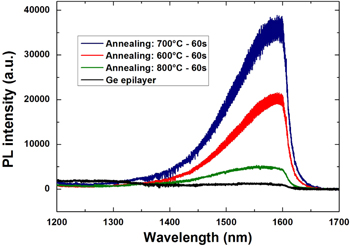
To investigate the effect of thermal annealing, i.e., to optimize the annealing parameters so that phosphorus atoms can be activated into the Ge substitutional sites, we display in figure 5 the evolution of the PL spectrum as a function of the annealing temperature of a sample doped with P at a substrate temperature of 170 °C. The annealing time was chosen to be of 60 s for all samples.
Figure 5. Dependence of the room-temperature PL spectrum on the thermal annealing condition. The highest PL intensity is obtained with annealing at 700 °C during 60 s.
Download figure:
Standard image High-resolution image
The figure reveals that the highest PL intensity is obtained for the annealing at 700 °C (dark blue curve). When the annealing temperature increases to 800 °C (green curve), the PL intensity is found to decrease. Such a decrease of the PL intensity can be attributed to the phosphorus out-diffusion to the surface and sublime in to the gas phase. Based on this result, we retain an adequate annealing temperature of 700 °C, and, in accordance with other experiments (not shown here) an annealing time from 30 to 60 s.
4. Conclusion
We have implemented an alternative n-doping process in Ge based on the decomposition of the GaP compound to produce P2 molecules, which have a higher sticking coefficient that that of P4 molecules. Throughout this study, we are able to set up numerous key parameters of the growth conditions, allowing us to obtain efficient emission of the Ge direct band gap at room temperature: the temperature of the doping GaP cell, the substrate temperature and the annealing condition. We have obtained an activated electron concentration up to 2 × 1019 cm−3, and more particularly an enhancement of the room-temperature PL intensity up to 50 times.
Acknowledgments
This work has been carried out thanks to the support of the A* MIDEX project (no ANR-11-IDEX-0001-02) funded by the 'Investissements d' Avenir' French Government Program, managed by the French National Research Agency (ANR).
It has also been partially supported by the ANR GRAAL project (Blanc 2011 BS03 004 01).
Footnotes
- *
Invited talk at the 7th International Workshop on Advanced Materials Science and Nanotechnology IWAMSN2014, 2-6 November, 2014, Ha Long, Vietnam.