

Abstract
Silicon nanowires have applications in various fields, e.g. vertical transistors, chemical or biological sensors, energy conversion, and storage devices. So far they have typically been obtained by bottom-up methods such as vapor–liquid–solid (VLS) synthesis, starting from metal nanoparticles. In this study, silicon nanowires are fabricated by dry reactive-ion etching using gold nanoparticles as a mask. Starting with the Bosch process, the cycle of SF6 plasma etching and C4F8 plasma deposition was optimized to control the quality of the resulting silicon nanowires.
Export citation and abstract BibTeX RIS

Original content from this work may be used under the terms of the Creative Commons Attribution 3.0 licence. Any further distribution of this work must maintain attribution to the author(s) and the title of the work, journal citation and DOI.
1. Introduction
Deep reactive-ion etching (DRIE) is a highly anisotropic etching process used to create deep holes and trenches in silicon wafers with a high aspect ratio and close-to-vertical sidewalls. Originally developed for the bulk micromachining of micro-electromechanical systems (MEMS) [1, 2], it is currently also used to create deep trenches for high-density capacitors in DRAM processing, and more recently for creating through silicon visa for 3D packaging [2–4].
The most common DRIE process is known as the Bosch process shown in [5, 6]. It is a form of PECVD process and includes the cycle of SF6 plasma etching and protecting the plasma of C4F8, each phase lasting a few seconds. The fluorocarbon passivation layer protects the entire substrate from further chemical attack and prevents uncontrolled etching. During the etching phase, the directional fluorosulfur ions which bombard the substrate etch away the passivation layer at the bottom of the trench faster than along the sidewalls. They subsequently sputter it off, exposing the substrate for the chemical reaction of silicon with the fluorosulfur species [5–8].
These etch/deposit steps are repeated many times in sequence resulting in a large number of very small isotropic etch steps taking place only at the bottom of the etched patterns. To etch through a 0.5° mm silicon wafer, for example, 100–1000 etch/deposit steps are needed. The two-phase process causes the sidewalls to undulate with an amplitude depending on the process parameters. The cycle time can be adjusted: short cycles yield smoother walls, and long cycles yield a higher etch rate [5, 6, 9, 10].
2. Experimental
A 3 μm diameter Au disk mask was created by standard photolithography, followed by electron-beam evaporation (see figure 1(a)). The mask thickness was about 25–30 nm.
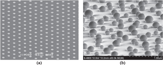
Figure 1. Photolithography defined (a) a 3 μm diameter gold mask and (b) gold nanoparticles created by thin film dewetting.
Download figure:
Standard image High-resolution imageAlternatively, Au nanoparticles (NPs) were created through the deposition of a thin film by electron-beam evaporation followed by rapid thermal annealing at 1100 °C for 30 s. The Au NP size depended on the thickness of the deposited Au thin film. We varied the size of the Au NPs from several tens to several hundred nanometers (see figure 1(b)).
The silicon substrate was subsequently DRIE-etched through the Au mask (figure 2). Observation was carried out using a field-emission scanning electron microscope (FE-SEM) and a 3D microscope of the resulting silicon nanowires.

Figure 2. Etching process to create Si NWs.
Download figure:
Standard image High-resolution imageThe Bosch process, named after the German company Robert Bosch GmbH which patented the process [5], also known as pulsed- or time-multiplexed- etching, alternates repeatedly between two modes to achieve nearly vertical structures. Starting with a nearly isotropic plasma etching, the plasma contains some ions which attack the wafer from a nearly vertical direction. Sulfur hexafluoride (SF6) is often used for the silicon. This is followed by the deposition of a chemically inert passivation layer—C4F8 (Octa fluorocyclobutane) source gas, for example, yields a substance similar to teflon [5–8].
Figure 3 shows the relationship between the main parameters of the etching process. The arrows help visualize the influence of the process parameters in relation to each other [11, 12].
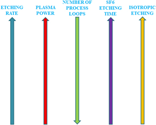
Figure 3. Relationship between the main parameters of the Bosch process.
Download figure:
Standard image High-resolution image3. Results and discussion
First, 3 μm diameter gold masks were used to determine the different ranges of RF power as well as the effect of bias voltage. This served as a reference to determine the parameters of the Bosch process for creating Si NWs using Au NPs as a mask.
3.1. Influence of the RF power
The RF power injected into the plasma was varied from 500 W to 100 W with the other parameters being kept constant (see table 1).
Table 1. DRIE parameters to determine the effect of plasma RF excitation source.
| Sample | RF power (W) | Number of etching loops | Duration of SF6/C4F8 plasma (s) | SF6/C4F8 flow rates (sccm) | Bias voltage (V) |
|---|---|---|---|---|---|
| A1 | 500 | ||||
| A2 | 300 | 200 | 5/10 | 100/150 | 200 |
| A3 | 100 |
Figure 4(a) shows that etching at 500 W did not allow the creation of Si NWs—only valley-like structures were obtained. High RF power etches away the Au mask very rapidly. By reducing the RF power to 300 W and keeping the etching time constant, the gold mask was nearly removed through isotropic etching by SF6 (figure 4(b)). Further reducing the RF power to 100 W allows the gold mask to be kept, and consequently, Si NWs were created (figure 4(c)). The thickness of the hard mask is determinant to achieving the proper formation of Si NWs.
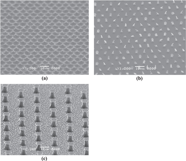
Figure 4. Silicon surface after etching with different amounts of RF power (a) 500 W, (b) 300 W, (c) 100 W.
Download figure:
Standard image High-resolution image3.2. Influence of the number of etching cycles and duration
As found above, the RF power was kept at 100 W. Two sets of parameters were tested: (i) 150 loops with SF6 etching for 4 s each, (ii) 300 loops with SF6 etching for 2 s each. Figure 5 shows that (i) results in a more isotropic etching. The gold mask was fully etched away for (i) while it remained relatively intact in (ii). For equal etching duration, the Si NWs present a controlled height in (ii).
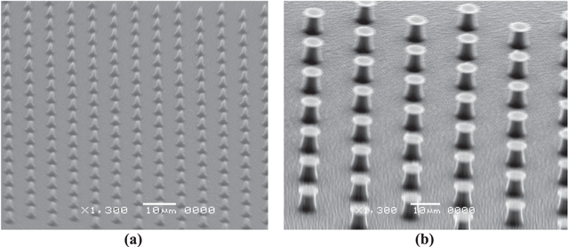
Figure 5. Silicon nanowires after (a) 150 loops with SF6 for 4 s, (b) 300 loops with SF6 for 2 s.
Download figure:
Standard image High-resolution imageReducing the etching time as well as increasing the number of etching loops improves the anisotropic etch for long SF6 plasma total duration.
3.3. Influence of the bias voltage
Here, the bias voltage was increased from 50 V to 200 V while other parameters were kept constant as in table 2.
Table 2. DRIE parameters to determine the effect of the bias voltage.
| Sample | RF power (W) | Number of etching loops | Duration of SF6/C4F8 plasma (s) | SF6/C4F8 flow rates (sccm) | Bias voltage (V) |
|---|---|---|---|---|---|
| C1 | 50 | ||||
| C2 | 100 | 200 | 5/10 | 100/150 | 100 |
| C3 | 150 | ||||
| C4 | 200 |
Observation under a 3D microscope (Sensofar, Spain) (figure 6) indicates that the bias voltage has an influence on the process leading to high anisotropy with increasing bias as shown in figure 7.
Table 3. DRIE parameters to create Si NWs with a Au NP mask at a SF6/C4F8 flow rate of 100/150 sccm.
| Sample | RF power (W) | Number of etching loops | Duration of SF6/C4F8 plasma (s) | Bias voltage (V) |
|---|---|---|---|---|
| D1 | 15 | 200 | 10/10 | 50 |
| D2 | 10 | 200 | 5/10 | 50 |
| D3 | 10 | 500 | 5/10 | 50 |
| D4 | 10 | 500 | 5/10 | 100 |
| D5 | 10 | 900 | 5/10 | 100 |

Download figure:
Standard image High-resolution image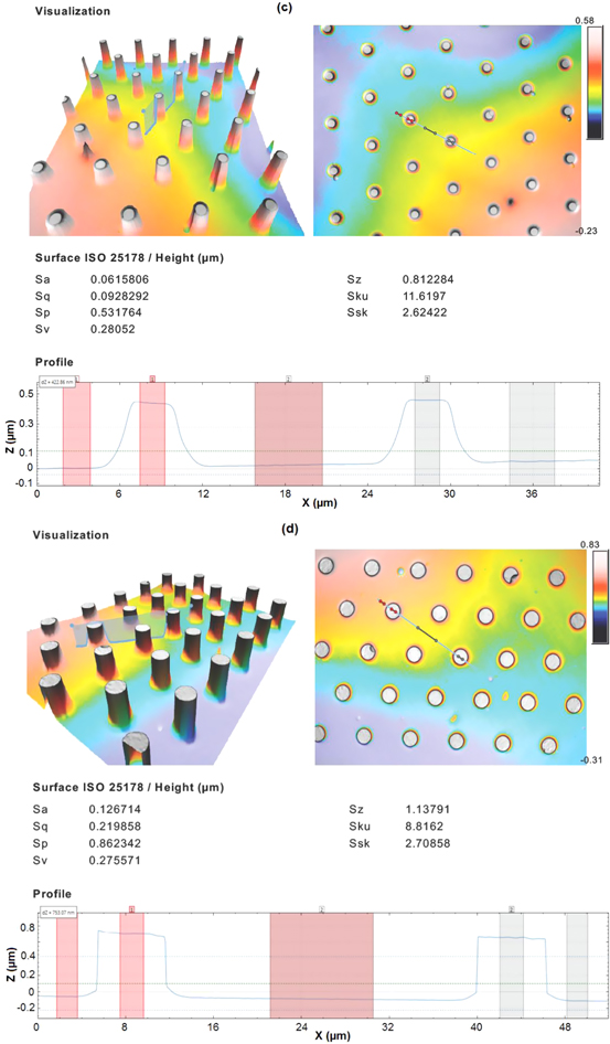
Figure 6. 3D microscope images of the four samples in table 2: (a) of sample C1, (b) of C2, (c) of C3 and (d) of C4.
Download figure:
Standard image High-resolution image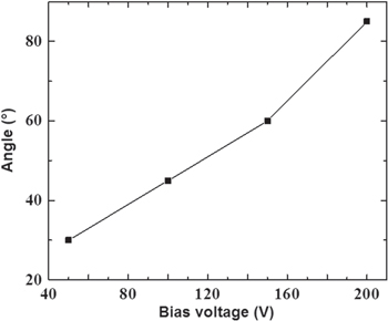
Figure 7. Angle between the wall of the structure and horizontal plane verticality as a function of bias voltage.
Download figure:
Standard image High-resolution imageA higher bias voltage in the etching step is very effective in decreasing passivation layer removal from the sidewalls as it directs the etching species more vertically towards the bottom of the etched patterns [13–15].
3.4. Creating Si NWs with Au NP masks
The above process optimisation using 3 μm Au masks was applied to the fabrication of Si NWs with Au NP masks (a few hundred nanometers in diameter) (detailed conditions in table 3).
The Si NWs obtained with sample D1 present an average diameter of 300 nm and an average height of about 3.1 μm (figure 8). However, a certain degree of isotropic etching is evident with a sidewall slope of about 70°. Reducing this angle necessitates the reduction in RF power as well as in the SF6 etching duration.

Figure 8. (a) FE-SEM image and (b) 3D topography of sample D1.
Download figure:
Standard image High-resolution imageFigure 9 presents the Si NWs obtained with sample D2, with the RF power at 10 W and the SF6 etching duration at 5 s with the number of process loops and other parameters kept identical with D1. The sidewall slope improved to 85° but the average height was now about 2.5 μm, a consequence of the reduction of RF power and SF6 etching duration. By increasing the total etching duration and increasing the etching loops to 500, the Si NW height is about 3.2 μm (figure 10).
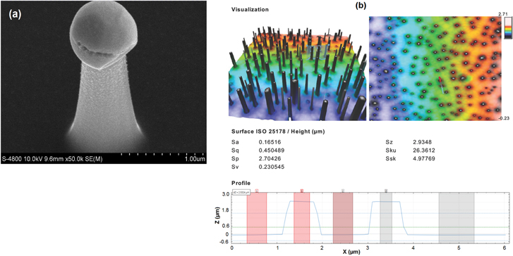
Figure 9. (a) FE-SEM image and (b) 3D topography of sample D2.
Download figure:
Standard image High-resolution image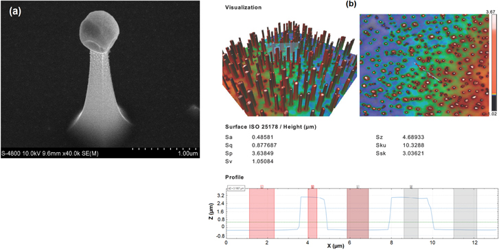
Figure 10. (a) FE-SEM image and (b) 3D topography of sample D3.
Download figure:
Standard image High-resolution imageSample D4 used the same process conditions as D3, except for a doubling of the bias voltage (figure 11). Although the height of the Si NWs was unchanged, the sidewall slope was significantly reduced. By increasing the number of etching loops to 900 (figure 12), 150–200 nm diameter Si NWs were obtained with a height of about 4 μm and a sidewall slope from 93° to 95°.

Figure 11. (a) FE-SEM image and (b) 3D surface of sample D4.
Download figure:
Standard image High-resolution image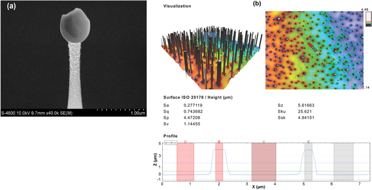
Figure 12. (a) FE-SEM image and (b) 3D surface of sample D5.
Download figure:
Standard image High-resolution image
4. Conclusion
In this study, the DRIE process parameters were optimized to obtain silicon nanowires using a gold nanoparticle mask. In particular, the influence of RF power, the number of etching loops, the SF6 etching duration and bias voltage were determined. We demonstrated the capability of this process for creating 150–200 nm diameter Si NWs with a height from 2.5 to 4 μm. The Si NWs walls are slightly tapered with a verticality of about 85°. The next step is to reduce the Si NW diameter using smaller nanoparticles that are a few tens of nanometer in size.
Acknowledgments
The authors gratefully acknowledge the Laboratory for Nanotechnology (LNT), Vietnam National University in Ho Chi Minh City (VNU-HCM) for supporting this study.