

Abstract
In this paper a two dimensional (2D) rectangular recessed channel–silicon on insulator metal oxide semiconductor field effect transistor (RRC-SOI MOSFET), using the concept of groove between source and drain regions, which is one of the channel engineering technique to suppress the short channel effect (SCE). This suppression is mainly due to corner potential barrier of the groove and the simulation is carried out by using ATLAS 2D device simulator. To have further improvement of SCE in RRC-SOI MOSFET, three more devices are designed by using dual material gate (DMG) and gate dielectric technique, which results in formation of devices i.e. DMRRC-SOI,MLSMRRC-SOI, MLDMRRC-SOI MOSFET. The effect of different structures of RRC-SOI on AC and RF parameters are investigated and the importance of these devices over RRC MOSFET regarding short channel effect is analyzed.
Export citation and abstract BibTeX RIS

Original content from this work may be used under the terms of the Creative Commons Attribution 3.0 licence. Any further distribution of this work must maintain attribution to the author(s) and the title of the work, journal citation and DOI.
1. Introduction
The restless evolution in the field of complementary metal–oxide–semiconductor (CMOS) technology has mainly been enabled by continuous and vigorously scaling of the device dimension in order to have smaller, faster, cheaper devices which leads to high speed and high packet density. Hence the over performance and functionality of the device increases with some constraints such as short channel effect (SCE), punch through effects, hot-carrier effect (HCE), threshold voltage roll-off (Vth roll-off), velocity saturation, drain inducing barrier lowering (DIBL), etc [1–3]. Due to the presence of these constraints there is performance degradation in the device.
In order to overcome this problem silicon on insulator (SOI) is consider as promising device to suppress SCE. SOI offers higher packet density. It consists of a buried oxide (BOX), which act as perfect insulator. Due to this insulating layer the active part of the device is completely isolated from the substrate. The presence of this BOX layer increases the overall performance of the device by reducing the junction capacitance, which in turn reduces the power consumption of the device and increases the device efficiency [4–6]. It is a latch-up free device, as it does not contain any well on the substrate. This leads to a reduction of leakage current. The speed of the device is also increased due to the reduction of parasitic capacitance.
With the passage of time various alternative techniques such as gate engineering and channel engineering have been proposed. One capable channel engineering technique is rectangular recessed channel metal oxide semiconductor field effect transistor (RRC MOSFET) [7–9]. It helps to solve most of the SCE and HCE problems. In RRC MOSFET, the source as well as the drain region is separated from one other with the help of a groove. Due to existence of this groove, the depletion region around the drain could not extend towards source and get pinched-off, which reduces the punch-through effect and SCE as well as enhances hot-carrier immunity [10]. Presence of this groove forms potential barriers each corner and these arise because of high electric field line, which is termed as corner effect. These potential barriers become sharper as well as higher for smaller corner radius and high substrate doping concentration [11, 12]. The channel formed around the groove of bent nature, due to the bend nature the saturation of drain current is less than that of convectional MOSFET. This corner effect is responsible for mitigating SCE, Vth roll-off and punch-through effect as well as HCE.
In this work, by combing the concept of rectangular recessed channel (RRC) and silicon on insulator (SOI) an improved structure has been proposed, known as RRC-SOI MOSFET. Here, the advantages of both the devices are taken into account in order to have better immune not only to SCEs , Vth roll-off, DIBL and punch-through effect as well as HCE from RRC, but also to have better sub threshold slope that will lead to less leakage current. Further improvement in the performance can be achieved by using the concept of gate engineering i.e. dual-material gate (DMG) technique and multilayer dielectric on RRC-SOI [13–21]. This leads to have more three devices i.e. dual-material rectangular recessed channel silicon on insulator (DMRRC-SOI), multilayer single-material rectangular recessed channel silicon on insulator (MLSMRRC-SOI) and multilayer dual-material rectangular recessed channel silicon on insulator (MLDMRRC-SOI) MOSFET, respectively. A systematic investigation of both DC performance such as drain current (ID), transconductance (gm), drain conductance (gd), output resistance (Rout), early voltage (VEA), intrinsic gain (AV), transconductance generation factor (TGF) and RF performances such as gate to source capacitance (Cgs), gate to drain capacitance (Cgd), cut-off frequency(fT) of the four device has been made.
2. Model simulation
The initial step in modeling the device is specifying the mesh on which the device will be constructed. The physical simulation domain is covered through a mesh or grid. The mesh is defined with a series of horizontal and vertical lines with spacing between them. To construct the device, different materials are assigned to the different regions within this mesh.
To analyze the device structure we apply the mathematical model of ATLAS 2D device simulator. It can be applied to various problems of semiconductor physics and consists of a set of fundamental equations which link together the electrostatic potential and the carrier densities. These equations, which are solved inside any general purpose device simulator, have been derived from Maxwell's laws and consist of Poisson's equation; the continuity equations and the transport equations. The electrostatic potential to local charge densities are described by Poisson's equation. The continuity and the transport equations describe the way that the electron and hole densities evolve as a result of transport processes, generation processes, and recombination processes.
A variety of physics models are used, such as Shockley–Read–Hall (SRH) model for recombination, constant voltage and temperature (CVT) model for inversion layer and parallel electric field-dependent mobility models for calculating carrier mobility [22].
2.1. Inversion layer mobility models
The mobility degradation that occurs inside inversion layers is taken into consideration to obtain accurate results for MOSFET simulations. The degradation occurs due to surface scattering near the semiconductor to insulator interface. The CVT model is designed to incorporate all the effects required for simulating the carrier mobility.
2.1.1. Lombardi CVT model
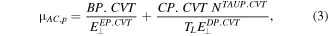
The inversion layer model from Lombardi is selected by setting CVT on the model statement. In the CVT model, the transverse field, doping dependent and temperature dependent parts of the mobility are given by three components. These components are μAC, μSr and μb where, μAC and μSr are related to interaction with an interface and are represented as:

where, the 1st component, μAC is the surface mobility limited by scattering with acoustic phonons. Surface mobility of electrons ( is given as
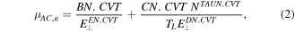
with BN.CVT, CN.CVT, DN.CVT, EN.CVT, TAUN are the default electron mobility parameters set by the simulator. TL is temperature, E⊥ is perpendicular component of electric field, N is total doping concentration. Similarly, surface mobility of holes ( is given as
with BP.CVT, CP.CVT, DP.CVT, EP.CVT, TAUP are the default hole mobility parameters set by the simulator.
The second component, μsr is surface roughness factor and given by:

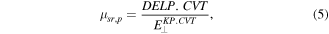
where DELN.CVT, KN.CVT , DELP.CVT, KP.CVT are the default electron and hole mobility parameters set by the simulator.
2.2. Parallel electric field-dependent mobility
As carriers are accelerated in an electric field their velocity will begin to saturate when the electric field magnitude becomes significant. Since the magnitude of the drift velocity is the product of the mobility and the electric field component in the direction of the current flow that shows the reduction of effective mobility. The following equations are used to implement a field-dependent mobility.
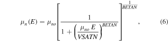

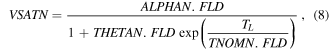
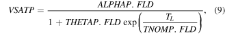
where E is parallel electric field, μn0 and μp0 are the low field electron and hole motilities, respectively. VSATN and VSATP are the C interpreter functions of the simulator. The BETAN and BETAP parameters are user-definable in the mobility statement.
2.3. Carrier generation-recombination models
Carrier generation-recombination is the process through which the semiconductor material attempts to return to equilibrium after being disturbed from it. If we consider a homogeneously doped semiconductor with carrier concentrations n and p to the equilibrium concentrations n0 an p0 then at equilibrium, a steady state balance exists according to mass action law,

The Shockley-Read-Hall (SRH) recombination has two following steps:
- An electron (or hole) is trapped by an energy state in the forbidden region which is introduced through defects in the crystal lattice. These defects can either be unintentionally introduced or deliberately added to the material, for example in doping the material; and
- If a hole (or an electron) moves up to the same energy state before the electron is thermally re-emitted into the conduction band, then it recombines.
The SRH recombination is modeled as follows:
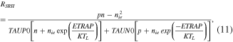
where ETRAP is difference between the trap energy level and the intrinsic Fermi level, TL is lattice temperature in degrees Kelvin, nie is intrinsic carrier concentration, TAUN0 and TAUP0 are the electron and hole lifetimes, which are user-definable in the material statement.
This model only presumes one trap level which, by default, is ETRAP = 0 and it corresponds to the most efficient recombination center. This model is activated by using the SRH parameter of the models statement.
3. Structure description and simulation
The schematic structure of RRC-SOI, DMRRC-SOI, MLSMRRC-SOI, and MLDMRRC-SOI MOSFET are shown in figure 1. These devices are designed by considering the total effective channel length of 102 nm during the design process i.e.

where Ls, Lp stands for angular and planar part of the groove respectively for both devices. The oxide thickness of 4 nm were taken around the gate. The source and drain regions are heavily doped with n type concentration of 1 × 1017 cm−3 and the substrate is doped with p type of concentration of 1 × 1020 cm−3. The thickness of the BOX which act as an insulating layer is consider as 100 nm and the other parameters specification considered to be identical to that of RRC model, as specified in table 1.
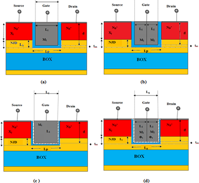
Figure 1. Schematic structure of (a) RRC-SOI, (b)DMRRC-SOI, (c) MLSMRRC-SOI and d) MLDMRRC-SOI MOSFET.
Download figure:
Standard image High-resolution imageTable 1. Device specifications used for different types of RRC-SOI structure ATLAS 2D.
| Device parameter | Dimension |
|---|---|
| Total effective channel length (Leff) | 102 nm |
| Negative junction depth (NJD) | 32 nm |
| Groove depth (d) | 80 nm |
| Corner angle (θ°) | 90° |
| Oxide thickness (tox) | 4 nm |
| BOX thickness (tbox) | 100 nm |
| Substrate doping (NA) | 1017 cm−3 |
| Source/drain doping (ND) | 1020 cm−3 |
| Lp | 38 nm |
| Ls | 32 nm |
| Junction depth (Xj) | 48 nm |
In case of MLSMRRC-SOI and MLDMRRC-SOI, the physical gate dielectric thickness, tox shown in figures 1(c) and (d) is divided into two parts

where tox1 and tox2 represent the oxide thickness of SiO2 and high-k, respectively, and the thickness  is considered, keeping the effective oxide thickness (EOT) intact. The electrical permittivities εox1 = 3.9 and εox2 = 10 are of SiO2 and high-k, respectively. In figures 1(b) and (d) two different materials having different work function has been merged into single gate to obtain an improved structure. Here the material M1 having higher work function has been placed near source side and the material M2 with lower work function is placed near the drain side. Out of the two materials, material M1 of length L1 serves as a controlling gate which produces an accelerating force to drive the charge carrier into the channel from the source side and other one, having length L2, serves as screening gate, which helps to suppress the SCEs and improvises ION current, transconductance (gm), cut-off frequency (fT). For both the device structures, the lengths L1 and L2 of materials M1 and M2 are consider the same i.e. L1:L2 = 1:1. The metal work functions of two materials are taken as qϕM1 = 4.06 eV and qϕM2 = 4.01 eV.
All the simulations of the four devices have been performed using ATLAS 2D simulator. The simulation has been performed using physical models accounting for the electric field-dependent and concentration-dependent carrier motilities with velocity saturation, SRH recombination/generation with doping dependent carrier lifetime, and Auger recombination. The mobility model used is the inversion layer Lombardi CVT mobility model, wherein concentration-dependent mobility, high field saturation model, and mobility degradation at interfaces are all included. The local electric-field-dependent model calculates mobility at every point in the inversion layer as a function of the net electric field at that point [22]. In this simulation all the junctions of the structure are assumed as abrupt and the biasing conditions are considered at room temperature.
4. Results and discussion
The variation of drain current of four different devices as a function of gate voltage at constant drain voltage is shown in the figure 2. From the figure it is clear that, MLDMRRC-SOI exhibits higher drain current as compared to the other proposed devices. The reason is that due to dual material, there is flow of uniform carrier in the channel which leads to high ION. Moreover the presence of multilayer dielectric results reduction in the leakage currents. So, combining both the factors results in better ION/IOFF. Similarly, figure 3 shows the output characteristic of four different structures. Here MLDMRRC-SOI shows higher drain current over all the models and that is due to better control of the gate over the channel and high mobility.
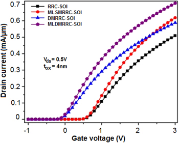
Figure 2. Variation of drain current (ID) with respect to gate voltage at constant Vds = 0.5 V.
Download figure:
Standard image High-resolution image
Figure 3. Variation of drain current (ID) with respect to drain voltage at constant Vgs = 1.2 V.
Download figure:
Standard image High-resolution imageTransconductance of a device determines the ability to amplify a signal. The greater the value of transconductance for any device, higher is the gain or amplification amount it can deliver. Figure 4 shows the variation of transconductance as a function of gate to source voltage for all the four devices. Since, the drain current of MLDMRRC-SOI exhibit higher value as compared to others, the transconductance of MLDMRRC-SOI is also higher. The main reason for enhancement of both ID and gm is due low doping concentration in the channel region and the peak electron velocity near the source region for the DMG devices.
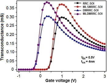
Figure 4. Variation of transconductance (gm) with respect to gate voltage at constant Vds = 0.5 V.
Download figure:
Standard image High-resolution imageSimilarly drain conductance determines the current driving capability of a device. Figure 5 shows the variation of the drain conductance (gd) with respect to drain voltage of the four different devices, where Vgs is kept constant at1.2 V. The performance of MLDMRRC-SOI as well as MLSMRRC-SOI exhibit better drain conductance and their values are almost close to each other. Whereas the value of MLDMRRC-SOI is slightly higher than of MLSMRRC-SOI due to slightly higher drain current which is shown in figure 3.
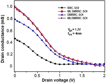
Figure 5. Variation of drain conductance (gd) with respect to drain voltage at constant Vgs = 1.2 V.
Download figure:
Standard image High-resolution imageFrom the figure 6, the variation of output resistance with the increase in gate voltage is shown. It is inversely related to the drain conductance i.e.  From the results, it is clear that MLDMRRC-SOI and DMRRC-SOI exhibits higher output resistance in comparison to MLSMRRC-SOI and RRC-SOI respectively. Such improvement in the device is due to the fact that the region of the channel which is under metal M2 provides a shielding effect in such a way that the variations of Vds could not affect the region of the channel under M1. This happens because Vds do not have any control on the drain current in the saturated region which leads to lower drain conductance and higher output resistance.

Figure 6. Variation of rout with respect to drain voltage at constant Vgs = 1.2 V.
Download figure:
Standard image High-resolution imageThe variation of the early voltage (VEA) with respect to drain bias for a constant gate voltage is shown in figure 7. The improvement of early voltage is seen in case of dual material (DM ) based devices as compared to single material (SM), due to reduction of SCE's. In the DM devices, M1 which is near the source controls the current driving capability, whereas M2 controls the output conductance. Hence the improvement of early voltage occurs because of balanced contribution from both the gates. MLDMRRC-SOI shows higher VEA than that any other device proposed the, whereas in the case of DMRRC-SOI, value of early voltage is higher than that of RRC-SOI. This value increases with the increase in the drain voltage mainly due to two factors. Firstly, due to DMG architecture which has been already discussed above and secondly due to presence of multi-layer gate oxide, the gate has better control over the charge carrier. As the total EOT which is offered by the high-k material is less, the value of early voltage increases and the dependence of transistor current on the Vds is reduced.
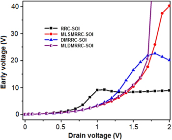
Figure 7. Variation of early voltage with respect to drain voltage at constant Vgs = 1.2 V.
Download figure:
Standard image High-resolution imageFigure 8 represents the variation of intrinsic gain (Av) with respect to Vds, at constant Vgs of 1.2 V. From the figure, MLDMRRC-SOI exhibits higher intrinsic gain than other devices. The improvement is seen due to high transconductance and low drain conductance. In order to have better performance in a device, both early voltage (VEA) and intrinsic gain (AV) should be very high.
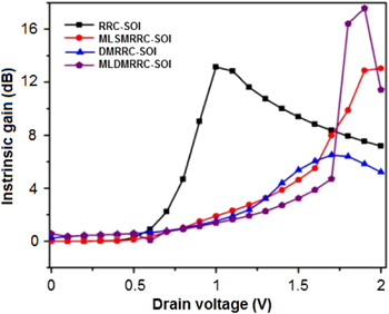
Figure 8. Variation of intrinsic gain with respect to drain voltage at constant Vgs = 1.2 V.
Download figure:
Standard image High-resolution imageTransconductance generation factor of a device determines the productive use of drain current to obtain an accepted value of transconductance  It is considered as an accessible gain per unit power dissipation. The ratio of gm/Id is considered to be maximum when it is in the weak inversion regime. Since, the drain current increases in the strong inversion regime there is sever degradation in a MOSFET or it can be said that its value increases in the sub-threshold region and it reduces as it approaches super-threshold region. For a device, having higher transconductance generation factors is considered to be highly efficient. The performance of the device increases as it can operate at low supply voltage. The variation of transconductance generation factor with respect to gate voltage is shown in figure 9. As RRC-SOI and MLSM RRC-SOI have positive threshold voltage (i.e. close to 0.4 V), its week inversion region occurs below this voltage, so the maximum TGF appears around Vgs of 0.0 V. Whereas in case of MLDMRRC-SOI and DMRRC-SOI the maximum TGF appears around Vgs of −0.8 V, as both the structure offers a negative threshold voltage nearly of −0.3 V. Among all the structure, by comparing the figures 2 and 4, the MLSM RRC-SOI offers higher value of TGF.
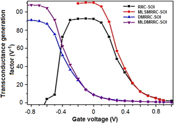
Figure 9. Variation of transconductance generation factor (TGF) with respect to gate voltage.
Download figure:
Standard image High-resolution imageThe capacitances Cgs and Cgd for different devices with respect to Vgs are shown in figures 10 and 11, respectively. The intrinsic gate capacitance is considered as an important parameter in RF analysis. Capacitances of all the four devices have been extracted from the small signal ac device simulations operating at a constant frequency of 1 MHz. Where the DC ramp voltage varies from −1 V to 2 V with a step of 0.1 V. The electron concentration is less at the source side as compared to the drain. This happens because the channel near the source side has higher threshold voltage due to the presence of higher work function material at the source end. The gate-to-source capacitance for DM devices is more prominent in the saturation region. Due to capacitance coupling between drain and gate electrodes, the Cgd for DM devices is higher. In case of MLDMRRC-SOI there is further increase in gate capacitance due to reduction of EOT. Here the physical oxide thickness of 4 nm is considered for all the models, keeping the thickness of both the dielectrics 2 nm each. When the high-k dielectric material is taken alone with gate oxide, the EOT for high-k gate oxide will be less as compared to SiO2. This leads to higher gate capacitance for high-k dielectric material as compared to SiO2. Since, the EOT of MLDMRRC-SOI is smaller as compared to others devices, there in an increase in total gate capacitance. From the plot it is clear that both Cgs and Cgd increases with the increase in Vgs until it reaches saturation. After the saturation level, the values of both the capacitances become constant as increase in Vds cannot affect the junction.
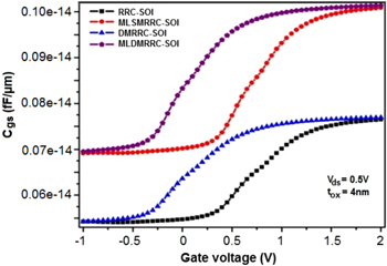
Figure 10. Variation of gate to source capacitance Cgs with respect to gate voltage at constant Vds = 0.5 V and frequency of 106 Hz.
Download figure:
Standard image High-resolution image
Figure 11. Variation of gate to drain capacitance Cgd with respect to gate voltage at constant Vds = 0.5 V and frequency of 106 Hz.
Download figure:
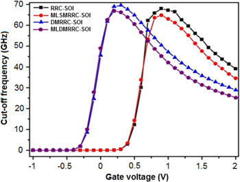
Standard image High-resolution imageCut-off frequency (fT) is one of the most important parameters for evaluating the RF performances of the device. The cut-off frequency, which is denoted as is the frequency where the current gain is equal to unity. The variation of cut-off frequency with respect to Vgs with constant Vds is shown in figure 12.
Figure 12. Variation of cut-off frequency with respect to gate voltage at constant Vds = 0.5 V.
Download figure:
Standard image High-resolution image
The cut-off frequency is obtained as

From the plot it observed that, MLDMRRC-SOI and MLSMRRC-SOI shows little reduction in the value of  as compared to DMRRC-SOI and RRC-SOI. This happens due to the use of high-k dielectric with SiO2. As the EOT of the gate oxide reduces, permittivity of high-k dielectric increases which in turn increases the total capacitance of the device. The value Cgs is very high as compared to
  Thus, the increase in transconductance can't compensate this increase in capacitance in order to obtain high cut-off frequency.
In order to analyze the short channel effect (SCE) of all devices, the extracted values of the threshold voltage (Vt), sub-threshold slope(SS) and drain induced barrier lowering (DIBL) are shown in the table 2. The term SS is defined as the change in gate to source voltage which must be applied to the device in order to produce one decade increase in the output current and calculated using the formula
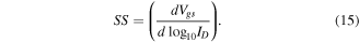
Table 2. Performance evaluation for different structure.
| Device type | Vt(V) | SS (V/decade) | DIBL | IDmax |
|---|---|---|---|---|
| RRC-SOI | 0.367 979 | 0.078 3724 | 0.311 070 | 0.000 508 71 |
| DMRRC-SOI | −0.282 984 | 0.079 2923 | 0.250 207 | 0.000 587 89 |
| MLSMRRC-SOI | 0.359 944 | 0.059 433 | 0.296 298 | 0.000 618 284 |
| MLDMRRC-SOI | −0.304 421 | 0.074 9877 | 0.262 452 | 0.000 706 43 |
SS is one of the important parameters in order to know about the OFF current. After implementing the concept of DMG and gate dielectric technique in RRC-SOI, it is clear that MLSMRRC-SOI exhibits better sub-threshold slope than others due to use of multi-layer dielectric. Where as in the case of MLDMRRC-SOI shows little higher SS value as compared to MLSMRRC-SOI due to use of DMG technique. As it shows higher voltage drop across the oxide at drain side due to slight increase in leakage current as compared to MLSMRRC-SOI. But if it is compared with the rest of the devices, MLSMRRC-SOI exhibits better SS.
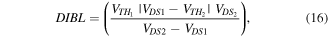
Similarly, DIBL is defined as the ratio of change in threshold voltage to the change in drain voltage and it is expressed by
where  and
and  are the threshold voltage of device which are obtained at
  and
and  respectively, and
  are two voltage applied to the same device. The extracted value shows that the device in which DMG technique is used provides a better DIBL. DMRRC-SOI shows lower DIBL among all the devices.
5. Conclusion
In this work the proposed 2D RRC-SOI MOSFET structure has been investigated using different types of technique such as DMG and gate dielectric technique and its performance improvement over the RRC- MOSFET has been studied using ATLAS-2D SILVACO software. From the results, it is cleared that DC performance parameter such as drain current, transconductance, output-conductance, output resistance, early voltage, intrinsic gain, transconductance generation factor and RF parameter such as intrinsic capacitance (Cgs and Cgd), cut-off frequency are improved as compared to RRC-SOI. Whereas in the case of evaluating SCE, it is seen that different of RRC-SOI designed provides better immunity to SCE (sub-threshold slope, threshold voltage, DIBL) as compared to RRC-SOI. Thus, the investigated device not only provides immunity to SCEs but also enhances the reliability of the device and performance in terms of the various factors stated above.