

Abstract
Analytical modeling with a verified simulation setup of surface potential, threshold voltage and electric field for a 4H-SiC MOSFET is presented to make enquiries about the short channel effects. The two-dimensional (2D) Poisson equation is used to achieve the model for surface potential. The 2D position equations have been solved by using four boundary conditions. The detail of the model is appraised by the various MOSFET parameters such as silicon carbide thickness, body doping concentration, and gate oxide influencing the electric field, channel potential and threshold voltage. The outcome shows that this model can reduce the short channel effects, drain induced barrier lowering and advance the sub-threshold fulfillment in nanoelectronic applications as compared to silicon MOSFETs. By comparing the model results with the 2D device simulations the veracity of the suggested 2D analytical model is proven.
Export citation and abstract BibTeX RIS

Original content from this work may be used under the terms of the Creative Commons Attribution 3.0 licence. Any further distribution of this work must maintain attribution to the author(s) and the title of the work, journal citation and DOI.
1. Introduction
Silicon carbide (SiC) was accidentally discovered in 1890 by E G Acheson, an assistant to Thomas Edison [1]. SiC is a compound semiconductor and is a mixture of silicon and carbon with the chemical formula SiC. Silicon is covalently bonded with carbon. In 4H-SiC, 4H is written in the Ramsdell classification scheme where the number indicates the layer and the letter indicates the Bravais lattice [2]. That means in a 4H-SiC structure four hexagonal layers of SiC are present. SiC exists in a kind of polymorphic crystalline building known as a polytype, e.g. 3C-SiC, 4H-SiC, 6H-SiC [2]. Presently 4H-SiC is usually preferred in power device manufacturing. SiC is a wider band-gap (Eg) material with Eg = 3.3 eV [3] as compared to silicon (Eg = 1.1 eV). Hence SiC has a band-gap three times higher than silicon. Due to its large bandgap, it has higher blocking voltage [3]. SiC is the most rising substrate for power MOSFETs and other power devices due to its high blocking voltage, great operating temperature, and admirable thermal conductivity. 4H-SiC MOSFETs are the power MOSFETs devices that have low switching losses and that can deliver low conduction with high breakdown voltages [4]. At the present time, SiC power MOSFETs with breakdown voltages from 500–1500 V [3] are readily available. SiC devices can also be made to have a much thinner drift layer, and greater doping concentration, i.e. the breakdown area for SiC is 2.4 MV cm−1 compared to silicon that has a breakdown discipline of 0.25 MV cm−1 [3]. That means the breakdown field for silicon is ten times lesser than SiC [4]. Electron mobility (μ) for SiC is 950 cm2 V−1 s−1 [4] compared to silicon, μ = 1400 cm2 V−1 s−1 [5]. This analogy shows that electron mobility for SiC is significantly less as compared to silicon. The continuous shrinkage of the device may require the attainment of excessive packing density and higher efficiency. However, the devaluation of the device dimensions in all forms decreases the performance that increases the high short channel effects. Compressing the bulk MOSFET into a nanometer MOSFET causes compelling challenges and difficulties with the control of the short channel effects [6–8]. According to our knowledge of concern, till now there is no analytical model on hand within the literature for the threshold voltage and surface potential of a nanoscale 4H-SiC MOSFET. The model presents the threshold voltage and surface potential of a nanoscale 4H-SiC MOSFET using the two-dimensional (2D) Poisson equation [9]. The 2D Poission equation may be solved by using the four boundary condition in the SiC region, and analyzing the behaviour of the threshold voltage [9, 10], surface potential, and electric field with varying device parameters like gate oxide thickness (tox), 4H-SiC thin layer thickness (t4H-SiC), channel length (L), and body doping (NA). The intention is to study a physics centered 2D model for a 4H-SiC MOSFET with the aid of solving the 2D Poisson equation [9]. Note that this model can be utilized as a useful tool for the characterization and design of high-efficiency 4H-SiC nanoscale MOSFETs together with the short channel peculiarities by varying various physical parameters. The validity of the model is checked by matching the model results with the 2D simulation results gathered utilizing T-CAD [11, 12].
2. Two-dimensional structure of a 4H-SiC MOSFET
The structure of the 4H-SiC MOSFET is shown in figure 1. When compared to a silicon MOSFET, the 4H-SiC MOSFET structure is especially helpful for device scaling. In this structure a 4H-SiC epilayer is grown on a silicon substrate. The epilayer is doped with the boron concentration of 1×1017 cm−3 [9]. The phosphorus concentration of 2 × 1020 cm−3 [9] is used for source and drain region doping. The silicon dioxide layer is maintained between the gate metal and the 4H-SiC layer and the thickness of the gate oxide layer is tox. All the device design parameters with specific values are tabulated in table 1. The compact model will be used for the characterization and design of high-efficiency nanoscale 4H-SiC MOSFETs.

Figure 1. Structure of a 4H-SiC MOSFET.
Download figure:
Standard image High-resolution imageTable 1. List of symbols and their description.
| Symbol | Confession | Numeric value |
|---|---|---|
| L | channel length | 100 nm |
| Eg,SiC | energy band gap of SiC | 3.25 eV |
| K | Boltzmann constant | 1.38 × 10⁻²³ |
| VT | the thermal voltage | 0.026 V |
| Eg,Si | band gap in Si | 1.1 eV |
| ΦM | metal gate work function | 4.35 eV |
| q | electron charge | 1.6 × 10⁻¹⁹ cm−3 |
| NA | body doping concentration. | 1 × 1017 cm−3 |
| N | source and drain doping concentration | 2 × 1020 cm−3 |
| Nb | substrate concentration | 1 × 1015 cm−3 |
| nSi | intrinsic carrier concentration in silicon | 1.45 × 1010 cm−3 |
| εSi | dielectric constant of Si | 11.7 |
| εSiC | dielectric constant of SiC | 9.7 |
| εox | gate oxide dielectric constant | 20 |
| tSi | silicon film thickness | 100 nm |
| tSiC | SiC thin film thickness | 30 nm |
| tox | thickness of gate oxide layer | 5 nm |
| ΦS(x) | surface potential in thin film | unknown |
| VGS | gate to source voltage. | 0.1 V |
| Vsub | the substrate bias | 0 V |
| VDS | drain to source voltage | 0.5 V |
| T | Temperature | 300 K |
2.1. Surface potential and electric field model
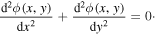
Before access of inversion let us write the 2D Poisson equation in the SiC thin film of a 4H-SiC MOSFET, presented in figure 1 as follows [9, 11, 13]
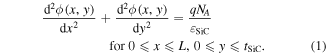
The surface potential profile in the SiC film will also be approximated by a parabolic function, as carried out in [9, 11, 13], i.e.

where the coefficients b1(x) and b2(x) are functions of variable x. Equation (1) may be solved by using the following four boundary conditions [9, 11, 13]:
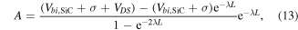
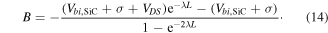
- (a) At the source side the surface potential is

with
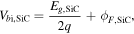
where  is the Fermi potential in SiC.
- (b) At the drain side the surface potential is

- (c) Electric field at the interface of the gate oxide and SiC film is continuous, i.e.

- (d) The electric field at the interface of SiC and the silicon substrate is

By using the boundary conditions (5) and (6), we can obtain the coefficients b1(x) and b2(x). Then by substituting these coefficients into the expression for ϕ(x, y) and setting y = 0, we obtain

where

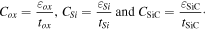
where Cox, CSi and CSiC, are the capacitances per unit area for the gate oxide layer, silicon layer and 4H-SiC film, respectively
The solution of equation (7) must satisfy the boundary conditions

and

Let us set  and
and  The second order inhomogeneous differential equation (7) with a constant coefficient has the following solution

where
2.2. Electric field model

2.3. Threshold voltage model
The threshold voltage model can be obtained by calculating the minima of the surface potential (12). From the condition

we obtain

The threshold voltage is the minimum value of gate to source voltage (VGS) at which a channel is established by the gate oxide at the surface of the 4H-SiC MOSFET. Therefore, in a 4H-SiC MOSFET, the threshold voltage is taken to be that value of VGS for which the surface potential is equal to twice the difference between the intrinsic and extrinsic Fermi level  [9, 10, 12–15]:

Here  is the value of the surface potential at which the inversion electron charge density in the 4H-SiC device is the same as the doping concentration. As a consequence, the threshold voltage is defined as the value of VGS at which the minimum surface potential
  is equal to
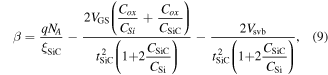
  Hence, accordingly, we will assess the value of the threshold voltage by substituting expression (16) into equation (17) and solving for equation (16) by putting the expressions of α, β, λ, σ, A and B

where
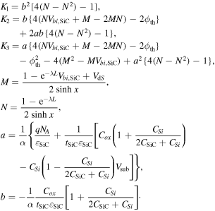
where K1, K2, K3, M, N, a, and b are constants and the expressions are as mentioned above and L being the channel length of the device.
Previously Mishra et al [16] have reported the analytical modeling of the potential profile of an SOI (silicon on insulator) tunnel FET by solving the 2D Laplace's equation, i.e.
In their approach the impact of space charge has been neglected because of the light doping profile of the channel. However, this work deals with the 2D Poisson's equation, i.e.
with consideration of the channel doping profile to evaluate the potential distribution, and the threshold voltage of the 4H-SiC MOSFET. Both the approaches consider the same boundary conditions, except the 4th case where they have calculated the electric flux at the channel and buried oxide interface (refer to equation (7) of [16]) and we have determined the electric flux at the channel/substrate interface as there is an SOI layer (refer to equation (6) of this work).
3. Results and discussion
3.1. Surface potential
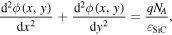
To validate the suggested analytical model, the 2D device simulator T-CAD [17] is used for the simulation of the surface potential distribution within the SiC layer and the threshold voltage (Vth) variation and the results are compared with the analytical model. Figure 2 shows the surface potential variation along the channel length for distinct values of drain voltages. It is understood from figure 2 that there is no powerful change in the potential at the source side and a very infinitesimal change at the drain side. As a final result, VDS has a very small effect on ID after saturation and it is visible from the figure that there is a negligible shift within the factor of the minimum surface potential regardless of the applied drain bias voltage. For this reason, drain-induced barrier lowering is substantially reduced for the 4H-SiC comparable to silicon. The model results and the simulation results [16] are correlated with each other to prove the accuracy of our suggested analytical model.
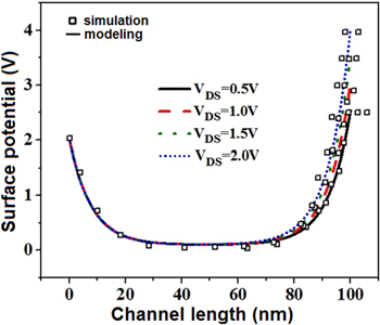
Figure 2. Graph for surface potential versus channel length for VDS = 0.5 V, VDS = 1.0 V, VDS = 1.5 V and VDS = 2.0 V. The device parameters are used as follows: Vsub = 0 V, VGS = 0.1 V, NA = 1 × 1017 cm−3, N = 2 × 1020 cm−3, tSiC = 30 nm, tox = 5 nm, tSi = 100 nm and ϕM = 4.35 eV.
Download figure:
Standard image High-resolution imageFigure 3 shows the surface potential variation along the channel for various values of oxide thickness. When the gate oxide thickness increased, the electric field decreased. Therefore, due to the fact that the decrement of electric field impact ionization also reduced, the rate of the generation of carriers was low. So, the controllability of the gate over the channel potential increases and it is less prominent to SCEs. Therefore, oxide thickness cannot be scaled right down to very small values due to the fact that the results of tunneling via the thin oxide and hot-carrier end up prominent.
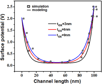
Figure 3. Graph for surface potential versus channel length for tox = 3 nm, tox = 6 nm, tox = 9 nm. The device parameters are used as follows: Vsub = 0 V, VDS = 0.5 V, VGS = 0.1 V, NA = 1 × 1017 cm−3, N = 2 × 1020 cm−3, tSiC = 30 nm, tSi = 100 nm and ϕM = 4.35 eV.
Download figure:
Standard image High-resolution imageFigure 4 shows the surface potential variation along the channel for various values of gate voltages. It may be observed from the figure that as the gate voltage increases, there is quite an increment in the height of the barrier at the source side and drain side. Therefore the surface potential increases in the channel region. Consequently, drain induced barrier lowering (DIBL) decreases and the immunity to manage the short channel effects (SCEs) is enhanced.
Figure 4. Graph for surface potential versus channel length for VGS = 0.1 V, VGS = 0.3 V, VGS = 0.5 V. The device parameters are used as follows: Vsub = 0 V, VDS = 0.5 V, NA = 1 × 1017 cm−3, N = 2 × 1020 cm−3, tox = 5 nm, tSiC = 30 nm, tSi = 100 nm and ϕM = 4.35 eV.
Download figure:
Standard image High-resolution image3.2. Electric field
Figure 5 shows the electric field distribution variation along the channel for distinct values of gate oxide thickness. It may be observed from the figure that at the drain side, with an increase in the gate oxide value, the electric field substantially reduces. Hence, the reduction of the electric field experienced by the carriers in the channel may be understood because of the reduction of the hot-carrier effect.
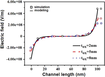
Figure 5. Graph for electric field versus channel length for tox = 2 nm, for tox = 5 nm, for tox = 8 nm. The device parameters are used as follows: Vsub = 0 V, VDS = 0.5 V, NA = 1 × 1017 cm−3, N = 2 × 1020 cm−3, tSiC = 30 nm, tSi = 100 nm and ϕM = 4.35 eV.
Download figure:
Standard image High-resolution image3.3. Threshold voltage
Figure 6 shows the variation of the threshold voltage along the channel for distinct doping concentration. As proven within the figure, the threshold voltage increases with improved body doping concentration. Hence, the scaling of the device can go to a further extent without any further increase in SCEs by increasing the body doping concentration. The threshold voltage obtained from the model correlates very well with the simulation result.

Figure 6. The graph for threshold voltage versus channel length for various values of NA. The device parameters are used as follows: Vsub = 0 V, VDS = 0.5 V, tSiC = 30 nm, tSi = 100 nm and ϕM = 4.35 eV.
Download figure:
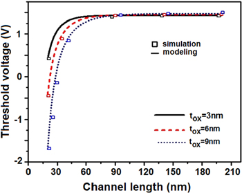
Standard image High-resolution imageFigure 7 shows the threshold voltage variation alongside the channel for distinct values of gate oxide thickness. When the gate oxide thickness is diminished, the threshold voltage can also be diminished which is the requirement for a faster device. Therefore, continuous scaling down of the gate oxide thickness offers a rise to faster devices. However, oxide thickness cannot be scaled all the way down to very small values because tunneling via the thin oxide layer and hot-carrier effects becomes prominent. It is clear that there is a close match between the analytical outcome and the 2D simulation outcome.
Figure 7. Graph for threshold voltage versus channel length for tox = 3 nm, tox = 6 nm, tox = 9 nm. The device parameters are used as follows: Vsub = 0 V, VDS = 0.5 V, VGS = 0.1 V, tSiC = 30 nm, tSi = 100 nm and ϕM = 4.35 eV.
Download figure:
Standard image High-resolution image
4. Conclusion
Analytical modelling of the electric field, surface potential and threshold voltage for a 4H-SiC MOSFET is developed based on the 2D physical model. The influence of quite a lot of device parameters like gate length scaling, body doping, SiC thickness, gate oxide thickness on the electric field, the surface potential, and the threshold voltage are analyzed. The results envisioned by the model are compared with the 2D simulations performed by using a commercially available device simulator SentaurusTM. There is a large drop in the threshold voltage with the decrease in channel length. The use of 4H-SiC material instead of silicon increases the device performance regarding reduced short channel effects. The compact model adequately predicts the threshold voltage over a gigantic variety of device parameters and can also be conveniently used to characterize and design the nanoscale 4H-SiC MOSFETs with the desired performance.