

Abstract
In this work we demonstrate an N-channel tunnel field effect transistor (TFET) i.e. double gate N-TFET for improved subthreshold slope (SS) and OFF-state leakage current (IOFF) with reference to drain bias (VDS), and body thickness (TSI). Device thickness is becoming a crucial parameter as more devices can built on thin film and integrate double or multi-gate MOSFETs. In this model we analyze the impact of VDS and TSI on the device performances and express the limitation of TSI with respect to ON-state current (ION), electric field, energy band diagram, etc. TFETs have become popular because these devices can operate in the sub-threshold region with the larger transconductance to current ratio (gm/Id) than MOSFETs, the current turn-on mechanism being interband tunneling rather than thermionic emission. The proposed model can achieve a subthreshold swing less than 35 mV/decade that is desirable for designing low-power high-frequency analog integrated digital circuit applications.
Export citation and abstract BibTeX RIS

Original content from this work may be used under the terms of the Creative Commons Attribution 3.0 licence. Any further distribution of this work must maintain attribution to the author(s) and the title of the work, journal citation and DOI.
1. Introduction
According to the present scenario, the limitation of power consumptions in modern CPU should not be beyond 100 W as shown in [1]. Nowadays, the tunnel field effect transistor (TFET) is one of the most promising devices for low power digital circuit applications [2]. TFETs are beneficial because they can be operated at a very low power supply, and are suitable for biomedical applications like biosensors, etc due to their low power operating region [3]. The power dissipation of any analog device can be observed from its subthreshold operation. In addition, the TFET is more efficient as a generator of transconductance in the subthreshold region.
In the subthreshold operation, the subthreshold slope (SS) relates to the transconductance to current ratio (gm/Id) as [4]

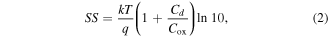
where gm is transconductance, and Id is drain current, Cd is depletion capacitance, Cox is oxide capacitance, k is Bolzmann constant, q is charge of electron, T is temperature (K).
In metal oxide semiconductor field effect transistors (MOSFETs), the gm/Id ratio is limited to values below 38.5 V−1 due to the restriction of SS to 60 mV/decade at room temperature (Cd ≪ Cox). But TFETs are free of this drawback of MOSFETs with a higher transconductance to current ratio (gm/Id) at room temperature [5]. This is because the TFETs can achieve SS values less than 60 mV/decade at room temperature. The importance of the gm/Id ratio is described in the following way: (1) it is strongly related to the performance of the analog circuits, (2) it also provides the operating region of the devices, and finally (3) it allows a tool for calculating the transistor dimensions like width, length, etc [6]. The working principle of the TFET is interband tunneling [7]; it means that the current injection mechanism of an N-channel tunnel field effect transistor (N-TFETs) is based on band to band tunneling (BTBT), i.e. an electron tunnels from the valence band of the source region into the conduction band of the intrinsic (channel) region.
Previously, Mishra et al [8] have proposed a single gate silicon on insulator (SOI) TFET by investigating the impact of the variation in TSI and gate oxide thickness (TOX) on the device characteristics and they have also analyzed various analog and RF parameters like electric field, transconductance (gm), drain conductance (gd), gate capacitance (Cgg), cut-off frequency (fT). However, this work mainly focuses on improving the SS, ON-state current (ION) by considering a double gate TFET (DG-TFET) device. The TSI is optimized by analysing the device characteristics and various performance parameters like the electric field, transconductance generation factor (TGF) and SS for the DG-TFET.
However, the only concern in TFETs is the ON-state current, which is very low as compared to conventional MOSFETs. Hence, there are many techniques used to improve the ON-state current without degrading the OFF-state current, such as (i) using a lower band gap semiconductor (SiGe, InGaAs, etc) at the source region [4, 9], and (ii) using high-k material, gate dielectric scaling, source and drain doping profile, which leads to an enhancement of the electric field (it improves the ON-state current) [10]. High-k spacer materials are widely used to enhance the device performance with more immunity towards the short channel effect (SCE) [11]. The design presented here is a DG N-TFET with a low-k gate dielectric to improve the drive current and ON–OFF ratio of the N-TFET. In order to evaluate the importance of TSI and optimize its value, we have performed the analysis of DG TFET with variations of TSI. In this paper, we have demonstrated that the ION is in the order of 10−6 A and IOFF is in the order of 10−18 A at VDS = 1.5 V with respect to different TSI. Due to its low ON-state and OFF-state currents, we can use this device for low-power complementary tunneling FET applications [12].
2. Device structure and simulation setup
The schematic layout and simulated device structure for an N-TFET are shown in figures 1 and 2, respectively. The device dimensions considered here are based on the International Technology Roadmap for Semiconductors [13], as shown in table 1. The source, drain, and intrinsic regions are formed with a specified dimension. A constant (or) uniform doping profile is used for all the regions, i.e. source, drain, and intrinsic regions. The source acts as a highly doped p-region with a concentration of 1020 atoms/cm3; the intrinsic region is lightly doped with a concentration of 1017 atoms/cm3 of n-type and the drain region acts as a highly n-type doped with a concentration of 1020 atoms/cm3. An insulated gate material made up of silicon dioxide (SiO2) with a dielectric constant of 3.9 is placed over the channel. The oxide thickness (TOX) of the gate dielectric is 1 nm. Here, TSI is considered as a variable ranging from 5–30 nm. To achieve better performance, the TSI is a beneficial parameter because it leads to better gate control and the reduction of the bulk capacitive effect. The source, drain, and gate contacts are made with metal, and the work function of the gate metal is chosen as 4.1 eV.

Figure 1. Schematic layout for N-TFET.
Download figure:
Standard image High-resolution image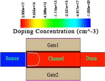
Figure 2. Simulated structure of DG-TFET with doping profile.
Download figure:
Standard image High-resolution imageTable 1. Design parameters considered for simulation.
| Parameter | Nomenclature | Double gate TFET |
|---|---|---|
| φM | Gate work function (eV) | 4.1 |
| NS | Source doping (cm−3) | 1020 |
| ND | Drain doping (cm−3) | 1020 |
| NC | Channel doping (cm−3) | 1017 |
| TOX | Oxide thickness (nm) | 1 |
| LT | Total device length (nm) | 150 |
| LG | Channel length (nm) | 50 |
| TSI | Silicon film thickness (nm) | 30, 10, 7, 5 |
For more accurate results, such as the ON-state current and OFF-state current, meshing is applied carefully for all the regions, i.e. source, drain and intrinsic regions. Two-dimensional simulations are done for double gate N-TFET using a commercially available device simulator Sentaurus TCAD [14]. For the device operation of N-TFET, a positive drain to source voltage (VDS) is applied. VDS is much less effective for the tunnel barrier width. But at a constant VGS when we increase the VDS, after a certain point, drain induced barrier narrowing is introduced, which leads to SCE in the TFETs. The current injection mechanism of an N-TFET is based on the BTBT of electrons from the valence band of the source region to the conduction band of the intrinsic region. In a TFET device, the tunneling of electrons takes place based on band bending in the channel region with an applied gate bias (VGS). When a positive VGS is applied, the energy bands of the channel or intrinsic region will be pushed down. Hence, if we apply more positive VGS, the tunneling barrier width becomes narrow so that electrons easily move from one band to another band, resulting in the improvement of drain current. The TFET is an ambipolar device, showing p-type behaviour with dominant hole conduction and n-type behaviour with dominant electron conduction. There are so many techniques analysed to overcome the ambipolar conduction in TFET [15, 16]. The results presented here are obtained by using a nonlocal BTBT model combined with the band gap narrowing model. Also, we have used Fermi–Dirac statistics and Shockley–Read–Hall recombination models [17, 18].
3. Results and discussion
The transfer characteristics (ID–VGS) of a double gate N-TFET with a channel length of 50 nm is shown in figure 3(a). From the characteristics, the variation of VDS does not make much difference for small values of VGS because the tunneling of electrons occurs based on the applied gate bias. The tunneling of electrons occurs when the value VGS is above the threshold voltage (VTh). The value of VTh obtained from the transfer characteristics is shown in table 2.
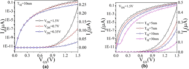
Figure 3. Device transfer characteristics for double gate N-TFET with a variations of VDS and silicon film thickness (TSI): (a) transfer characteristics for different values of VDS; (b) transfer characteristics for different values of TSI.
Download figure:
Standard image High-resolution imageTable 2. Performance analysis of double gate TFET.
| Parameter | Nomenclature | TSI = 5 nm | TSI = 7 nm | TSI = 10 nm | TSI = 30 nm |
|---|---|---|---|---|---|
| VTh (V) | Threshold voltage | 0.431 | 0.452 | 0.472 | 0.491 |
| SS (mV dec−1) | Subthreshold slope | 25.458 | 28.407 | 33.227 | 46.941 |
| ION (μA) | ON-state current | 0.453 | 0.310 | 0.237 | 0.102 |
| IOFF (pA) | OFF-state current | 1.104 × 10⁻⁴ | 8.215 × 10⁻⁶ | 1.703 × 10⁻⁶ | 4.366 × 10⁻⁵ |
| ION/IOFF | ON–OFF ratio | 4.09 × 10⁹ | 37.7 × 10⁹ | 139 × 109 | 2.35 × 10⁹ |
In TFETs, drain current under high gate and drain bias can be expressed by equation
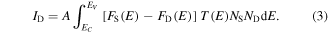
It is possible because the channel quasi-Fermi level is in equilibrium with the drain Fermi level at high gate and drain bias. In equation (3), T(E) is the electron tunneling probability, because the ON-state current is proportional to the electron tunneling probability. FS(E) and FD(E) are the source and drain side Fermi–Dirac distributions, responsibility, and NS and ND are the corresponding density of states, A is the area of the device. The integral range from EC (channel) to EV (source) represents the range of energies over which tunneling takes place. The Wentzel–Kramers–Brillouin expression for tunneling probability is shown in
where Eg represents the barrier height seen by the particle touching the tunnel barrier (band-gap of the material in this case), m* is the effective mass of the tunneling particle (material dependent) and F is the maximum electric field at the tunnel junction. It means that the lower band-gap, low mass materials (low Eg and m*) and higher electric fields will result in higher ON-state currents [19]. The maximum TGF can be expressed as
where Eg is the barrier height, VGS is the gate to source voltage.
Further, we consider the results with the variation of TSI at a particular drain to source voltage, i.e. VDS = 1.5 V. The results are depicted in figure 3(b), as we decrease the TSI, the ON-state current improved with a reference of 10 nm, and when TSI increases, the ON-state current is reduced. It means that a smaller value of TSI has better electrostatic control of the dual gate over the channel, which helps to eliminate the SCE. With an aligned gate dielectric, the improved electrostatics lead to an increase of the ON-state current and lower threshold voltage as well as lower SS when the silicon film thickness is made thinner. However, some limitations are observed with a decrease of TSI below 10 nm, i.e. the IOFF current degrades (as shown in table 2), due to the quantum mechanical effects [20, 21]. The Schrödinger formulation of quantum mechanics deals with the particle tunneling through an energy barrier, as with the propagation of evanescent electromagnetic waves [22]. The extremely narrow potential well is created for the lower TSI values because of the strong sub-band splitting and carrier confinement in the vertical direction [23].
Also, from the characteristics, we can state that the IOFF current is very low and the SS obtained is 25 mV/decade that are very small compared to conventional MOSFET [4]. The parameters extracted from the transfer characteristics are tabulated as shown in table 2 at VDS = 1.5 V.
In TFETs, the electric field plays a very vital role in improving the ON-state current of the devices. As given in equation (5), when the electric field increases at the tunnel junction, the tunneling of the electron probability is improved that accelerates the drain current. There are many methods introduced to improve the electric field at the tunnel junction, such as: (1) gate dielectric scaling, (2) the realization of devices on ultrathin SOI structure, (3) underlap drain structure, and (4) source and drain doping profile.
As the tunnel width decreases with increasing VDS, it results in an increase of the electric field at the tunnel junction. The variation of the electric field with VDS is shown in figure 4(a). Similarly, as the value of TSI decreases, the electric field of the tunnel junction is improved, as can be seen from figure 4(b). This is because of the inversely proportional nature of the electric field to the TSI according to the relation given in equation (5).
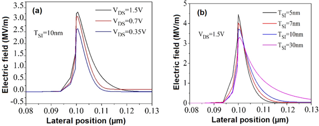
Figure 4. The electric field behavior analysis of double gate N-TFET. The electric field variations (a) with different VDS, and (b) with different silicon film thickness (TSI).
Download figure:
Standard image High-resolution imageWith the help of the energy band diagram, the ON–OFF state phenomenon of the double gate N-TFETs is explained in figure 5. As shown in figure 5(a), when VGS = 0.0 V and VDS = 1.0 V, the tunnel barrier width is more and the height is less, so electrons do not have enough energy to move from the valance band of the source to the conduction band of the channel. This phenomenon is known as the OFF-state. As shown in figure 5(b), when VGS = 1.0 V and VDS = 1.0 V, the barrier width is less and the height is more; at the VDS > VTh the electrons have sufficient energy to move from one band to another band. This phenomenon is known as interband tunneling or ON-state.

Figure 5. Simulated electron energy band diagram for double gate N-TFET with separation between the source, channel, and drain region. (a) OFF-state at VGS = 0.0 V and VDS = 1.0 V; (b) ON-state at VGS = 1.0 V and VDS = 1.0 V.
Download figure:
Standard image High-resolution imageFigure 6 shows that the energy barrier width is dependent on the applied VGS as well as VDS. The barrier width is maximum at VGS = 0 V, and as we increase the applied gate bias, the barrier width is reduced. However, at high values of VGS, the barrier width starts to saturate. Hence, for the limited value of VGS, the barrier width is effected and elsewhere it is constant.

Figure 6. The energy barrier width of the double gate N-TFET variation with respect to VGS at TSI = 10 nm.
Download figure:
Standard image High-resolution imageTunneling region (barrier height and width) is not much affected by the variation of VDS for a constant TSI, as shown in figure 7(a). As TSI is decreased, the change in energy levels becomes less gradual from the source to the drain, as can be observed from figure 7(b). This analysis confirms the existence of a charge-neutral region, meaning that the surface region of the channel is less depleted of electrons because increasing the VDS results in less resistance in the tunnel junction. Thus, the ON-state current is improved. If we compare the electric field and band diagram, it concludes that the electric field is more, where the energy band is a steeper slope; elsewhere the electric field is approximately negligible.

Figure 7. Simulated electron energy band diagram for double gate N-TFETs: (a) energy band diagram change with respect to different values of (a) VDS, and (b) silicon film thickness (TSI).
Download figure:
Standard image High-resolution imageFigure 8 shows the transconductance of a double gate N-TFET with the variation of VDS and TSI. The transconductance increases by decreasing the TSI. This happens due to the interrelation of transconductance to drain current (ON-state). From the above analysis, we have observed that the ON-state current is inversely proportional to the TSI. The transconductance is also an important parameter for analog applications like gain, and the cut-off frequency of any device [24, 25].

Figure 8. The analog performance of the double gate N-TFET: transconductance variation with different values of (a) VDS and (b) silicon film thickness (TSI).
Download figure:
Standard image High-resolution imageFigure 9 shows the output or drain characteristics of the double gate N-TFET by varying VGS and TSI. The output characteristic is improved and the threshold value is decreased with decreasing TSI. The current achieves its optimum for TSI = 5 nm.
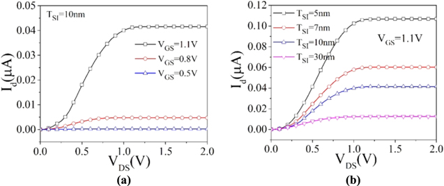
Figure 9. Device output characteristics for double gate N-TFET: the output characteristics for different values of (a) gate voltage (VGS) and (b) silicon film thickness (TSI).
Download figure:
Standard image High-resolution imageThus the transconductance generation factor (TGF) of TFETs is very high as compared to conventional MOSFETs. The maximum TGF, i.e. (gm/Id)max is calculated with the help of equation (5) and the values of device thickness are presented in table 3.
Table 3. The maximum variation of transconductance generation factor (gm/Id)max at different silicon film thickness TSI (obtained from equation (5)).
| TSI (nm) | (gm/Id)max (V−1) |
|---|---|
| 5 | 1320 |
| 7 | 1140 |
| 10 | 486 |
| 30 | 263 |
Table 3 shows that the device thickness TSI = 5 nm gives larger (gm/Id)max values than the other values of TSI. Such large values have been beneficial in the design of the circuits meant for analog applications.
The effect of TSI on the SS as well as on drain induced barrier lowering (DIBL) is shown in figure 10. Their performances are improved by the reduction of TSI and that results in better gate control on the channel and also reduces SCEs.
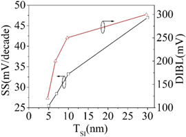
Figure 10. The subthreshold slope (black line) and DIBL (red line) is a function of double gate N-TFET silicon film thickness (TSI).
Download figure:
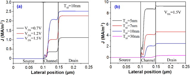
Standard image High-resolution imageFigure 11 shows the current density plot at fixed VGS = 1.0 V and varying VDS as well as TSI of the double gate N-TFET. The current density is more at the drain region as compared to the channel region because, at higher VDS, the accumulation of electrons is decreased at the channel region. By increasing VDS, the maximum number of electrons is more depleted from the source region than at the channel region. On the other hand, we have observed that the current density increases as we decrease the TSI because the electron concentration per unit area will be increased.
Figure 11. Current density plot for double gate N-TFET at different values of (a) drain voltage (VDS) and (b) silicon film thickness (TSI).
Download figure:
Standard image High-resolution image
4. Conclusion
In this paper, we have proposed TFETs that can operate at a very low subthreshold region with a higher transconductance generation factor (gm/Id) and a lower TSI. Details of the investigation have been carried out for a double gate N-TFET with reference to TSI and VDS. By using the device with proper process parameters and biasing conditions, we can design low power analog circuits. For a TSI of 5 nm, a high ON-state current can be achieved, which helps to increase the operating speed of the device. It is also compatible with lower DIBL so that it is less sensitive towards SCEs.