

Abstract
Electrical conductivity of zinc oxide nanoparticles (ZnO NPs)-decorated bacterial nanowires is investigated in the present work. The ZnO NPs are prepared through a simple precipitation method and characterized by UV–vis spectrophotometer, Fourier transform infrared spectroscopy, x-ray diffraction, atomic force microscopy (AFM), scanning electron microscopy (SEM) and high resolution transmission electron microscopy (HRTEM). The SEM analysis discloses that the prepared ZnO NPs are spherical in shape with an average particle size of 3.5 nm. The ZnO NPs are decorated on the surface of bacterial nanowires and the same are characterized by AFM and HRTEM. The electrochemical performance of the bare bacterial nanowires and ZnO NPs-decorated bacterial nanowires is analyzed by cyclic voltammetry and linear sweep voltammetry, whereas their electrical conductivity is measured by electrochemical impedance spectroscopy. The results of the electrochemical investigations indicate that the ZnO NPs coating on the surface of bacterial nanowires improve the electrical conductivity of the bacterial nanowires.
Export citation and abstract BibTeX RIS

Original content from this work may be used under the terms of the Creative Commons Attribution 3.0 licence. Any further distribution of this work must maintain attribution to the author(s) and the title of the work, journal citation and DOI.
1. Introduction
The biological role of extracellular appendages may vary among microorganisms [1] and the extracellular electron transport is accomplished by conductive filamentous extracellular appendages called bacterial nanowires [2–5]. The bacterial nanowires were first explored in Pseudomonas aeruginosa and their subsequent analysis by atomic force microscopy (AFM) demonstrated transverse electrical conductivity property. The bacterial nanowires derived from other microorganisms, including gram negative bacteria, such as Vibrio anguillarum and Vibrio alginolyticus were also exhibited similar kind of transverse electrical conductivity property [6]. The isolation and separation of bacterial nanowires from these bacteria species were already established [7]. The morphological and conductivity analysis of these bacterial nanowires were carried out by AFM. It was reported that the individual bacterial nanowire had a diameter of 80 nm and a length of 1–10 μm [3].
Nanosized metal oxide semiconductors have gained immense attention in recent years, owing to their desirable properties with diverse applications, such as catalysts [8], sensors [9], photoelectron devices [10, 11], highly functional and effective devices [12]. These semiconductor nanomaterials have novel electronic, structural and thermal properties, which are all have high scientific interests in basic and applied fields. Owing to the diverse properties and functionalities, the nanosized metal oxide semiconductors are regarded as one of the most versatile classes of materials. The nanosized metal oxide semiconductors possess unique properties that can be acquired towards the invention of novel and efficient nanodevices. In this respect, rapid research developments have been made pertaining to nanosized metal oxide semiconductors. The study of nanosized metal oxide semiconductors has attracted huge attention, due to their peculiar size and shape dependent properties for electronic applications. Consequently, numerous investigations have been carried out to control the morphology of nanosized metal oxide semiconductors [13–15]. Among the different nanosized metal oxide semiconductors, ZnO NPs have been much investigated as potential monooxide material for both fundamental investigations and practical applications [16–20]. In recent years, ZnO NPs have been applied for different fields of application like photocatalyst [21], photoanode [22] and multifunctional application [23].
The ZnO NPs have been employed in a range of optoelectronic applications because of their unique electrochemical and optical properties [24]. The photophysical features of ZnO NPs are acquired to develop several sensor and biosensor systems [25–27]. Among the different semiconductor materials applied to develop biosensors, ZnO has an advantage of large bandgap energy (3.3–3.6 eV) that encompasses both photoconductivity and photocatalytic properties [28].
Due to the unique physical, electrical and structural properties of ZnO NPs, in the present work we choose them to decorate the surface of bacterial nanowires with the aim of enhancing their electrical conductivity. The present investigation demonstrates the preparation of ZnO NPs-decorated bacterial nanowire nanocomposites through an eco-friendly and cost-effective route. The physiochemical and electrochemical characterization of the ZnO NPs-decorated bacterial nanowires are studied in detail. The electrochemical properties are systematically demonstrated for the bare as well as ZnO NPs decorated bacterial nanowires by electrochemical techniques, such as cyclic voltammetry (CV), linear sweep voltammetry (LSV) and electrochemical impedance spectroscopy (EIS). The electrical properties of the ZnO NPs-decorated bacterial nanowires are comparable to that of the moderately doped inorganic semiconductors and their elasticity are similar to polymeric materials. Hence, the bacterial nanowires derived from microorganisms may function as building blocks for bionanoelectronics and flexible nanoelectronics.
2. Materials and methods
2.1. Chemicals and reagents
Zinc sulfate heptahydrate and sodium hydroxide were purchased from Merck. All other chemicals used in this work were belonging to analytical reagent grade obtained from Merck. Millipore water was used for the preparation of solutions. Double distilled water, purified by Nanopure® water system was employed for the preparation of solutions towards electrochemical experiments.
2.2. Preparation of ZnO NPs
The ZnO NPs were prepared through a simple precipitation method according to a reported procedure [29]. Briefly, sodium hydroxide aqueous solution was drop-wise slowly added to zinc sulfate aqueous solution at a molar ratio of 1:2 under vigorous stirring and the stirring process was continued for 12 h. The white precipitate thus obtained was filtered and washed thoroughly using millipore water through centrifugation. Then, the precipitate was collected and redispersed in millipore water for removing excess ions. Finally, the precipitate was gathered, dried at 100 °C in a hot air oven and grounded to fine powder with the aid of agate mortar.
2.3. Characterization of ZnO NPs
Adsorption feature of the ZnO NPs was recorded in the UV–vis wavelength range between 200 and 800 nm by diffuse reflectance spectral (DRS) accessory equipped in a UV–vis spectrophotometer (UV 2500 Shimadzu). Fourier transform infrared (FTIR) spectroscopy of the ZnO NPs was recorded using Shimadzu 8201 PC. The spectral region between 4000 and 400 cm−1 was scanned and KBr disc method was employed for recording the FTIR spectrum. X-ray diffraction (XRD) pattern of the ZnO NPs was taken in an x-ray diffractometer (XPERT-PRO), operated at a voltage of 40 kV and a current of 30 mA with Cu-Kα radiation (λ = 1.540 60 Å). The XRD pattern was recorded between the 2θ range of 10° and 80° in a fixed time mode at room temperature. AFM images of the ZnO NPs were recorded in a Shimadzu SPM 9500-2J scanning probe microscope. The roughness of the ZnO NPs was measured from the AFM images. The surface morphology of the ZnO NPs was analyzed through scanning electron microscopy (SEM) images. The SEM images were recorded using SU-70 (ModelL-HI-0028-0001) SEM operated at an applied voltage of 10 kV. The surface morphology of the ZnO NPs was examined through high resolution transmission electron microscopy (HRTEM). The HRTEM images of the ZnO NPs were taken in a FEI-200 KeV, LaB6 filament, Tecnai T20 G2 TEM system.
2.4. Preparation of ZnO NPs-decorated bacterial nanowire film
Isolation, characterization and electrical conductivity measurement of bacterial nanowires were performed according to our previous report [5, 7]. Briefly, the ZnO NPs decorated bacterial nanowires was obtained by mixing 0.5 mg of ZnO NPs in 1 ml of bacterial nanowires suspension, in which the ZnO NPs were decorated on the surface of bacterial nanowires subject to mild shaking. A known volume (10 μl) of the ZnO NPs–bacterial nanowires suspension was casted on a pre-cleaned glass plate surface which was allowed to dry at room temperature. The resultant thin film was used for AFM characterization.
2.5. Morphological characterization of ZnO NPs-decorated bacterial nanowires
The surface morphology of ZnO NPs-decorated bacterial nanowires was analyzed through AFM and HRTEM.
2.6. Conductivity measurement of ZnO NPs-decorated bacterial nanowires
2.6.1. CV and LSV studies
Electrochemical experiments were performed in a CHI 660B electrochemical work station (CH Instruments Inc., USA), equipped with a conventional one-compartment three-electrode cell. A glassy carbon (GC) electrode with an active area of 0.07 cm2 was used as a working electrode, a silver/silver chloride electrode (Ag/AgCl) was employed as a reference electrode and a platinum coil was adopted as a counter electrode. The GC electrode was polished twice using alumina powder (0.05 μm particle size), followed by sonication in double distilled water for 3 min and the same was employed towards modification of the GC electrode. All the experiments were carried out in a deaerated 0.1 M H2SO4 solution.
2.6.2. Electrochemical impedance spectroscopy measurements
Electrochemical experiments were carried out in a CHI 660B electrochemical work station (CH Instruments Inc., USA), using a conventional one-compartment three-electrode cell. A cleaned GC substrate electrode was used as a working electrode with an active surface area of 0.07 cm2, a silver/silver chloride (Ag/AgCl) electrode was employed as a reference electrode, and a platinum coil was used as a counter electrode. The GC electrode substrate was cleaned in acetone by sonication for 10 min and subsequently cleaned in double distilled water for 10 min Argon (Ar) gas was purged into the solution to establish an oxygen (O2) free environment. All the electrochemical experiments were performed at room temperature.
EIS responses were obtained at GC electrodes modified with bacterial nanowires and metal oxide coated bacterial nanowires. The redox analyte used was 1 mM K3Fe(CN)6 in 0.1 M KCl. The electrode was polarized at 0.25 V with the frequency range of 1 Hz–100 kHz. We employed [Fe(CN)6]3−/4− couple as a redox probe to study electrical conductivity behavior of the bacterial nanowires and ZnO NPs decorated bacterial nanowires. The Nyquist diagram of the complex impedance represents imaginary versus real part of the impedance spectrum. The Nyquist plot shows a semicircle at higher frequencies corresponding to electron-transfer-limited process and linear portion at lower frequencies corresponding to diffusion-limited process.
3. Results and discussion
UV–vis DRS of the ZnO NPs is shown in figure 1. The DRS exhibits a strong characteristic absorption band of ZnO at 365 nm [30] and moreover, its sharp absorption feature indicates that the ZnO NPs are monodispersed in nature [31]. The chemical constitutions of the ZnO NPs were examined through FTIR spectroscopy in the range of 500–4000 cm−1 at room temperature (figure 2). The band at around 3394 cm−1 is ascribed to the existence of hydrogen-bonded O−H stretching, while the bands at 1381 and 1419 cm−1 are due to the presence of C–H stretching and C–H bending, respectively. These bands are occurred owing to the presence of residual zinc sulfate, which was used during the synthesis of ZnO NPs [32]. The band at 2928 cm−1 is indication of C−H mode, while the bands 1465 and 1647 cm−1 are corresponding to the C–H bending and –C=C–stretching mode, respectively. The peak at 482 cm−1 is attributed to the absorption peak of Zn–O bond and also authenticates the presence of ZnO. Figure 2 corresponds to the wurtzite oxide stretching frequencies of ZnO. The major absorption band at ∼450–500 cm−1 is the stretching mode of ZnO [33, 34].
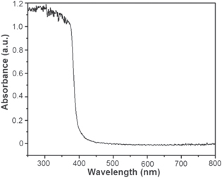
Figure 1. Absorption spectra of the ZnO NPs.
Download figure:
Standard image High-resolution image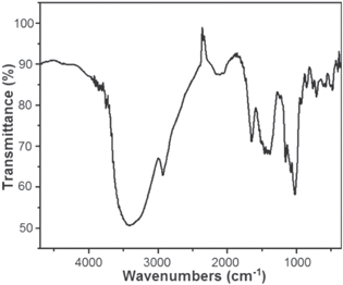
Figure 2. FTIR spectrum of the ZnO NPs.
Download figure:
Standard image High-resolution imageXRD analysis was carried out to elucidate crystalline nature of the prepared ZnO NPs as it provides characteristic diffraction pattern of crystallites under particular configuration through Bragg's law. Figure 3 shows the XRD pattern of the synthesized ZnO NPs. The characteristic diffraction peaks of ZnO NPs are appeared at 2θ values of 31.63°, 34.37°, 47.39°, 56.49°, 62.84°, 67.87°, 69.02° and 76.82°, which are corresponding to the crystalline diffraction planes of (110), (002), (101), (102), (110), (103), (112), (201) and (202), respectively. These indicate that the ZnO NPs are made up of wurtzite hexagonal structure [35]. All the diffraction peaks agree with the standard JCPDS card no. 36-1451. According to the XRD results, the ZnO NPs possess high crystallinity, due to their very sharp diffraction peaks. Moreover, any other additional impurity peaks are not detected in the XRD pattern, which implies the high purity of synthesized ZnO NPs.

Figure 3. XRD pattern of the ZnO NPs.
Download figure:
Standard image High-resolution imageThe morphology of ZnO NPs characterized by the AFM images are shown in figure 4. It can be realized from the AFM images that the ZnO NPs are spherical in shape. The roughness of the ZnO NPs examined by the AFM is depicted in figure 5. For the ZnO NPs, the roughness peak attained a maximum height of 2.2 nm with an average maximum roughness peak height of 1.8 nm, a maximum roughness valley depth of 3.7 nm and an average maximum roughness valley depth of 2.1 nm. Figure 6 shows the SEM image of ZnO NPs, which indicates that the synthesized ZnO NPs are well-dispersed and spherical in shape. To elucidate the dispersion of ZnO NPs, low-magnification (figure 6(a)) and high-magnification (figure 6(b)) SEM images were taken. The high-magnification SEM image reveals that the surface of every ZnO NPs is rough and each NPs is built up of numerous small clusters of ZnO NPs. Meanwhile, the small size of the ZnO NPs is previously evidenced by the HRTEM images. The HRTEM images of ZnO NPs with different magnification were also recorded (figures 7(a)–(d)). As clearly seen in the high-magnification HRTEM image (figure 7(d)), the ZnO NPs are spherical in shape with an average particles size of 3.5 nm.
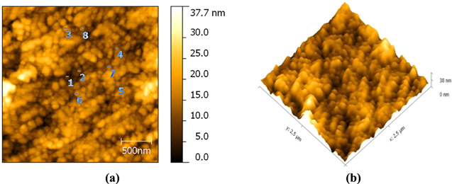
Figure 4. AFM images of ZnO NPs (a) 2D image and (b) 3D image.
Download figure:
Standard image High-resolution image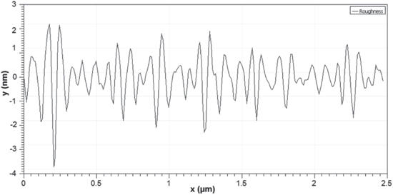
Figure 5. Roughness of ZnO NPs measured by AFM.
Download figure:
Standard image High-resolution image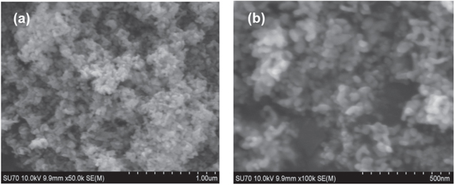
Figure 6. SEM images of ZnO NPs with low- (a) and high- (b) magnifications.
Download figure:
Standard image High-resolution image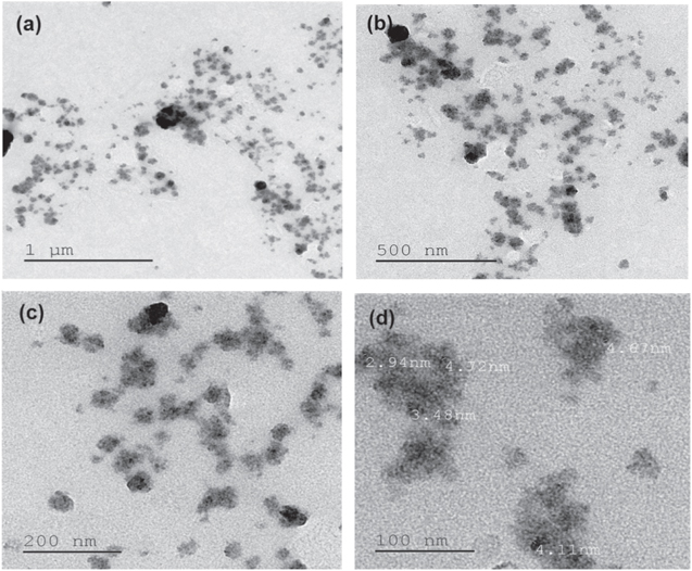
Figure 7. HRTEM images of ZnO NPs with different magnifications (a)–(d).
Download figure:
Standard image High-resolution imageFigure 8 displays the AFM micrographs of ZnO NPs decorated bacterial nanowires. The AFM micrographs visibly illustrated the coating of ZnO NPs on the surface of bacterial nanowires. If the size of bacterial nanowires gets increased, more surface area became available for ZnO NPs deposition on the bacterial nanowires. This led to the increase in the thickness as well as surface roughness of the ZnO NPs which were decorated on the surface of bacterial nanowires. However, surface roughness is uniform for particular concentration of bacterial nanowires. In addition, the HRTEM images were recorded for the ZnO NPs decorated bacterial nanowires. The surface decorated ZnO NPs were viewed in the presence of 0.5 mg ml−1 bacterial nanowires (figures 9(c) and (d)). It is observed from the HRTEM images that the size and shape of the ZnO NPs are changed after their decoration on the surface of bacterial nanowires. The ZnO NPs can bind on the surface of the bacterial nanowires and can effectively improve the interaction between nanoparticles as shown in figure 10.
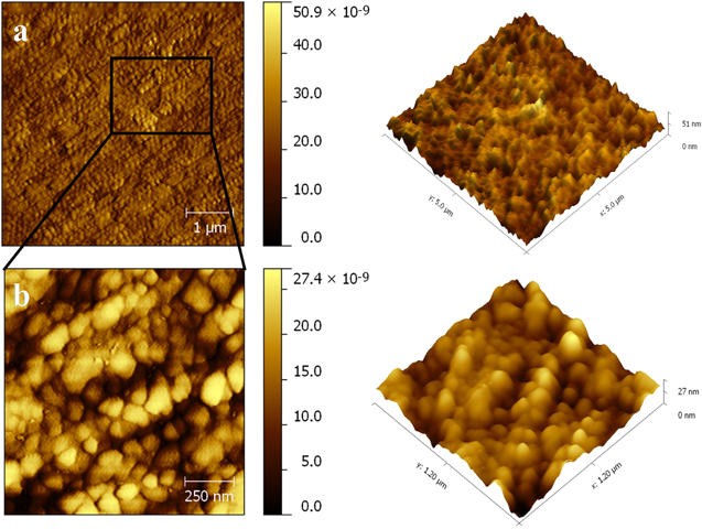
Figure 8. AFM images of ZnO NPs decorated bacterial nanowires at different magnifications (a), (b).
Download figure:
Standard image High-resolution image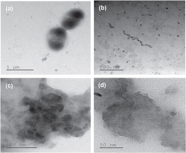
Figure 9. HRTEM images of (a) Pseudomonas aeruginosa bacterial cells, (b) separated bacterial nanowires, (c) and (d) bacterial nanowires decorated by ZnO NPs at different magnifications.
Download figure:
Standard image High-resolution image
Figure 10. Schematic representation of ZnO NPs decorated bacterial nanowires for electrochemical applications.
Download figure:
Standard image High-resolution imageFigure 11 shows the cyclic voltammograms recorded for the bare bacterial nanowires and ZnO NPs decorated bacterial nanowires. Figure 11(a) depicts the CV of the bacterial nanowires modified GC electrode recorded at a scan rate of 20 mV s−1 by immersing the GC electrode in an electrolyte solution of 0.1 M H2SO4. The GC electrode modified by the bacterial nanowires exhibited a well-defined redox electrochemical behavior. The anodic peak was obtained at around 0.3 V (versus Ag/AgCl), while the cathodic peak was observed at around 0.34 V. It is evident that the bacterial nanowires accept electrons from the metal center and gives them to oxygen [2]. In addition, this reaction generates a passive oxide layer at the protein/metal interface. Figure 11(b) illustrates the CV of GC electrode modified by ZnO NPs decorated bacterial nanowires. As per our expectation, the capacitance of the GC electrode was significantly decreased by the coating of ZnO NPs on the bacterial nanowires. Moreover, the redox peaks were reduced with a positive shift. After complete dispersion of ZnO NPs on the surface of bacterial nanowires, the redox peaks may be concealed. Thus, the protection effect of metal oxide nanoparticles layer seems to be related to its passivation effect, as well as its barrier behavior. The decrease in the capacitance current suggested that the conductivity of the bacterial nanowires was increased by decorated them with ZnO NPs. The CV of the ZnO NPs decorated bacterial nanowires exhibited a more positive value. In this case, the ZnO NPs decorated bacterial nanowires act as more effective conductivity barrier for bacterial nanowires [36]. The positive shift of ZnO NPs coated bacterial nanowires depressed the anodic current and as a consequence, they offered greater resistance [37]. As a result, the introduction of ZnO NPs concentration on the surface of bacterial nanowires led to exhibit high potential properties. It can be revealed that both the electrochemical properties and barrier effects increase potential of the composite coatings. The electrochemical property is caused by increase in the potential and the formation of a passive layer on the surface of bacterial nanowires.
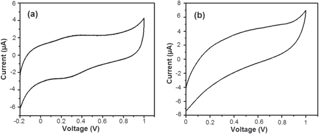
Figure 11. CVs of bacterial nanowires modified glassy carbon electrode (a) and ZnO NPs decorated bacterial nanowires modified glassy carbon electrode (b) recorded in 0.1 M H2SO4, at a scan rate of 20 mV s−1.
Download figure:
Standard image High-resolution imageThe direct electrochemistry of the GC electrode modified bare bacterial nanowires and ZnO NPs decorated bacterial nanowires electrodes were investigated by LSV. The electrochemistry of the ZnO NPs-coated bacterial nanowires showed highest conductivity when compared to the bare bacterial nanowires (figure 12). The onset of current flow was observed at the breakdown voltage range from 0.1 to 1.0 V. The results indicated that the presence of ZnO NPs on the bacterial nanowires surface had exhibited great electrochemical response, which can be ascribed to the excellent characteristics such as good electrical conductivity and high surface area of the ZnO NPs-decorated bacterial nanowires. The suitable electronic properties of the ZnO NPs-decorated bacterial nanowires provided the ability to promote charge transfer reactions. This observation suggested that the ZnO NPs-decorated bacterial nanowires are appropriate for use in electrochemical applications.

Figure 12. Linear sweep voltammetry curve of ZnO NPs decorated bacterial nanowires (curve (a)) and bacterial nanowires (curve (b)) recorded in 0.1 M H2SO4, at a scan rate of 20 mV s−1.
Download figure:
Standard image High-resolution imageFigure 13 shows the Nyquist impedance curves of the GC electrodes modified by bacterial nanowires both in the presence and absence of ZnO NPs which were obtained in a mixed electrolyte solution of 1 mM K3Fe(CN)6 and 0.1 M KCl. These Nyquist impedance curves were fitted well to the corresponding circuit models. The equivalent circuit models consist of solution resistance (Rs), charge transfer resistance (Rct), constant-phase element for double layer (CPEdl) and CPE for the coating film (CPEc). Here, the CPE was used instead of the capacitance (C) to define the homogeneity of the system [38, 39]. The obtained Rs values were in the range of 83–87 Ω. The observed Rct values were 2800 and 1900 Ω for bare bacterial nanowires and ZnO NPs-decorated bacterial nanowires, respectively. The CPE values were 0.93 and 0.87 for bacterial nanowires and ZnO NPs-decorated bacterial nanowires, respectively, and the obtained values were close to one, which were considered to be double layer capacitance. The film resistance value obtained for the ZnO NPs-decorated bacterial nanowires was relatively low with respect to bare bacterial nanowires, which might be related to the electronic distribution channels of ZnO NPs-decorated bacterial nanowires [40]. The charge-transfer resistance value of ZnO NPs-decorated bacterial nanowires was lower than that of the bare bacterial nanowires, which was associated with the surface morphology of ZnO NPs-decorated bacterial nanowires. The introduction of ZnO NPs on the surface of bacterial nanowires lead to decrease in the resistance for charge transfer during electrochemical reaction. The film capacitance of ZnO NPs-decorated bacterial nanowires was found to be higher than that of the bare bacterial nanowires. The results revealed that the ZnO NPs-decorated bacterial nanowires had better conductivity and charge storage capability [40]. Some authors reported that the nanosize additives improve the anticorrosion electrochemical barrier layer properties of polymers for diffusion of solvent [41–43]. The increased surface area of bacterial nanowires in the reaction medium is one of the advantages of the polymerization of bacterial nanowires in the presence of nanoparticles. One of the special properties of electroactive nanowires is their ability to interact with the liberated ions during the corrosion reaction of steel in the presence of chloride ions [44–46]. Hence, their performance increases with increasing surface area.

Figure 13. EIS recorded for ZnO NPs decorated bacterial nanowires. Redox analyte is 1 mM of K3Fe(CN)6 in 0.1 M KCl. The electrode was polarized at 0.25 V and the frequency range was 1 Hz–100 kHz.
Download figure:
Standard image High-resolution image
4. Conclusion
Bacterial nanowires and ZnO NPs-decorated bacterial nanowires were successfully prepared and characterized by different physicochemical and electrochemical methods. The AFM images exhibited that the incorporation of ZnO NPs on the surface of bacterial nanowires affected their morphology and as a consequences they increased the surface area of the bacterial nanowires. Moreover, the presence of ZnO NPs within the coating on the surface of bacterial nanowires enhanced their potential effect. The relatively decreased charge transfer resistance value and the capacitance of ZnO NPs-coated bacterial nanowires electrodes revealed that the ZnO NPs-coated bacterial nanowires exhibited high conductivity in comparison to bacterial nanowires electrode. The composite of the ZnO NPs-decorated bacterial nanowires system opens the avenue for the future designs of various metal oxide/bacterial nanowires composites for electrochemical technological applications.
Acknowledgments
The authors are grateful to University Grants Commission (F.No.39-559/2010 (SR), dt.12.01.2011), Government of India, New Delhi and DST PURSE Scheme, Madurai Kamaraj University for their financial support. The authors express their thanks to the University with Potential for Excellence (UPE) Scheme, Madurai Kamaraj University for generously providing instruments facility.