

Abstract
By utilizing pulsed laser deposition (PLD), heterojunctions comprised of n-type nanocrystalline (NC) FeSi2 thin films and p-type Si substrates were fabricated at room temperature in this study. Both dark and illuminated current density–voltage (J–V) curves for the heterojunctions were measured and analyzed at room temperature. The heterojunctions demonstrated a large reverse leakage current as well as a weak near-infrared light response. Based on the analysis of the dark forward J–V curves, at the V value ⩽ 0.2 V, we show that a carrier recombination process was governed at the heterojunction interface. When the V value was > 0.2 V, the probable mechanism of carrier transportation was a space-charge limited-current process. Both the measurement and analysis for capacitance–voltage–frequency (C–V–f ) and conductance–voltage–frequency (G–V–f ) curves were performed in the applied frequency (f ) range of 50 kHz–2 MHz at room temperature. From the C–V–f and G–V–f curves, the density of interface states (Nss) for the heterojunctions was computed by using the Hill–Coleman method. The Nss values were 9.19 × 10¹² eV−1 cm−2 at 2 MHz and 3.15 × 10¹⁴ eV–1 cm–2 at 50 kHz, which proved the existence of interface states at the heterojunction interface. These interface states are the probable cause of the degraded electrical performance in the heterojunctions.
Export citation and abstract BibTeX RIS

Original content from this work may be used under the terms of the Creative Commons Attribution 3.0 licence. Any further distribution of this work must maintain attribution to the author(s) and the title of the work, journal citation and DOI.
1. Introduction
Several researchers have reported that semiconducting iron disilicide (β-FeSi2) comprising nontoxic elements (Si and Fe) has attracted much attention recently as a new promising candidate for application in silicon-based optoelectronic devices [1–4]. It is because β-FeSi2 possesses both indirect and direct optical bandgaps of 0.74 eV, and 0.85 eV, respectively. These optical bandgap values are of relevance to optical fiber telecommunication wavelengths [5–7]. Additionally, β-FeSi2 grown epitaxially on Si with small lattice mismatches [8–10] has an optical absorption coefficient of more than 105 cm−1 at 1.2 eV [11–13]. Nanocrystalline (NC) FeSi2 grown on any solid substrate at room temperature possesses semiconducting features close to β-FeSi2 [14–16]. It is comprised of a crystal with diameter range of 3–5 nm [17] and has a larger optical absorption coefficient than β-FeSi2 [18, 19]. Thus, NC-FeSi2 is an attractive material for application in silicon-based optoelectronic devices.
In a previous study, NC-FeSi2 thin films grown by utilizing pulsed laser deposition (PLD) were investigated for their structural and electrical features [17]. The NC-FeSi2 thin films possessed n-type conduction and a carrier density ranging between 1018 to 1019 cm−3 [17]. After that, the near-infrared (NIR) light detection performance for the n-type NC-FeSi2/p-type Si heterojunctions fabricated utilizing PLD was studied [14]. Based on the experimental results, the fabricated heterojunctions demonstrated a large reverse leakage current and a weak NIR light response at room temperature. A probable cause was likely the existing interface states at the heterojunction interface between NC-FeSi2 and Si acting as a center of leakage current and a trap center for photo-generated carriers [14–16]. However, the estimations of the density of interface state (Nss) and the probable transportation mechanisms of the carrier at the heterojunction interface between NC-FeSi2 and Si have not been studied in detail yet.
In the present study, the measurement and analysis of capacitance–voltage–frequency (C–V–f ) and conductance–voltage–frequency (G–V–f ) curves of the n-type NC-FeSi2/p-type Si heterojunctions fabricated by utilizing PLD were performed at room temperature. The Nss value at the heterojunction interface between NC-FeSi2 and Si was computed by utilizing the Hill–Coleman method. It proved the existence of interface states for the heterojunctions in this study. These interface states probably are the cause of the degraded electrical properties in the aforementioned heterojunctions. Additionally, the probable transportation mechanism of the carrier through the heterojunction interface was studied. At V ⩽ 0.2 V, the predominant transportation mechanism of the carriers was the recombination process. It was governed by a space-charge-limited current (SCLC) process at V > 0.2 V. According to the available knowledge of the authors, this study is the first investigation of the Nss value and probable transportation mechanisms of the carrier at room temperature for the n-type NC-FeSi2/p-type Si heterojunctions fabricated utilizing PLD.
2. Experimental details
NC-FeSi2 thin films with a thickness of 100 nm were grown on a p-type Si(1 1 1) substrate at room temperature by means of PLD by utilizing a FeSi2 target. The oxide layer was initially removed from the substrate by utilizing hydrofluoric acid (HF) and then cleaned with deionized water. The cleaned substrate was instantly mounted on a substrate holder in a PLD chamber. The PLD chamber had a base pressure of 10–6 torr. The distance of the substrate to the FeSi2 target was fixed at 50 mm. An argon fluorine (ArF) laser beam with a wavelength of 193 nm was focus onto the rotating FeSi2 target using a spherical lens. The repetition rate of the laser pulses was 10 Hz and fluence was 10 J cm−2. A radio frequency magnetron sputtering apparatus was used to form the back and front ohmic contacts of the heterojunctions. Pd films were formed on the back of the Si in a finger-shaped pattern, whereas Al films were formed on the whole NC-FeSi2. A schematic diagram of the n-type NC-FeSi2/p-type Si heterojunctions formed utilizing PLD is shown in figure 1.

Figure 1. Schematic diagram for n-type NC-FeSi2/p-type Si heterojunctions fabricated utilizing PLD.
Download figure:
Standard image High-resolution imageThe crystalline structure for the NC-FeSi2 thin films grown on Si substrate was characterized by utilizing x-ray diffraction (XRD; Rigaku RINT2000/PC). Observation of the surface morphology of the NC-FeSi2 thin films grown by PLD was performed by using the Carl Zeiss Auriga field emission scanning electron microscope (FESEM) at Facility Building 10 (F10), the Center for Scientific and Technological Equipment, Suranaree University of Technology. The NC-FeSi2 thin films grown by PLD were also observed by transmission electron microscopy (TEM; JEM-2000EX Conventional TEM) at the Ultramicroscopy Research Center, Kyushu University [17]. The measurement of the current density–voltage (J–V) curves for the heterojunctions was performed by utilizing a Keithley 2400 source meter at room temperature in the dark and under the illumination of a 6 mW of 1.31 µm laser diode. The measurements of C–V–f and G–V–f curves were carried out with a LCR meter (Agilent E4980A) at room temperature with the f value range of 50 kHz–2 MHz. From the C–V–f and G–V–f curves, the series resistance (Rs) value was computed by utilizing the Nicollian–Brews method and the Nss value was computed by utilizing the Hill–Coleman method.
3. Results and discussion
The typical XRD patterns of the NC-FeSi2 film deposited on a Si(1 1 1) substrate by PLD and Si(1 1 1) substrate (background) are shown in figure 2. The measurement was performed utilizing a grazing incidence method (2θ scan) at a fixed incidence angle of 4°. For comparison, the XRD pattern of the NC-FeSi2 film deposited on a Si(1 1 1) substrate by facing targets direct-current sputtering (FTDCS) was measured in the same manner shown in figure 2. The XRD pattern of the NC-FeSi2 film deposited by PLD shows a broad peak in the 2θ range between 40 and 50° [14, 17], which is similar to that of NC-FeSi2 film deposited by FTDCS [15]. In this range, orthorhombic β-FeSi2 has several crystalline planes for diffraction, such as 331, 313, 040, 004, 041, 114, 511, 422, and 133. Thus, the broad peak is likely owing to the nanocrystalline structure of the NC-FeSi2 film, which resulted from the overlapping of diffraction peaks for these crystalline planes [14, 15, 17]. Due to the robust quenching of highly-energetic species on the surface of the substrate, the nucleation of β-FeSi2 immediately takes place in the PLD process. Nanocrystallites comprising the NC-FeSi2 film should be nuclei formed in the mentioned process [14]. The broad peak of NC-FeSi2 film deposited by PLD is weak compared with that of NC-FeSi2 film deposited by FTDCS. Because the quenching effect in the PLD process is stronger than that in the FTDCS process, the NC-FeSi2 film deposited by PLD comprises of smaller crystallites. In other words, it would be closer to amorphous FeSi2 film [15].

Figure 2. XRD patterns for NC-FeSi2 film deposited by PLD and FTDCS (for comparison), which were measured by utilizing a grazing incidence method (2θ scan) at a fixed incidence angle of 4°.
Download figure:
Standard image High-resolution imageFigure 3(a) shows a FESEM image of the NC-FeSi2 thin films grown by PLD. From the obtained FESEM image, the NC-FeSi2 thin films have a very smooth surface and consist of numerous crystallites with diameters of 4–5 nm. Figure 3(b) displays the dark-field image of NC-FeSi2 thin films using the broad ring [17]. The NC-FeSi2 thin films consist of a large number of small crystallites with diameters ranging from 3 to 5 nm. This result corresponds to the FESEM image.

Figure 3. (a) FESEM image of surface morphology for NC-FeSi2 thin films grown on Si substrate by utilizing PLD at room temperature, and (b) dark-field image of NC-FeSi2 thin films grown on Si substrates by using PLD [17].
Download figure:
Standard image High-resolution imageFigure 4 demonstrates the room temperature J–V curves of n-type NC-FeSi2/p-type Si heterojunctions under reverse and forward bias voltage conditions, in the dark and under illumination of a 6 mW, 1.31 µm laser light. The heterojunctions demonstrated a rectifying action similar to that observed in conventional pn abrupt junctions. However, the heterojunctions demonstrated a large reverse leakage current. In addition, the illuminated current under reverse bias voltage increased slightly compared with that of dark current. These results were probably because of the existing interface states at the heterojunction interface between NC-FeSi2 and Si acting as a center of leakage current and a trap center for the photo-generated carriers [14–16].

Figure 4. The dark and illuminated J–V curves for n-type NC-FeSi2/p-type Si heterojunctions fabricated utilizing PLD at room temperature.
Download figure:
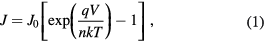
Standard image High-resolution imageThe study of the dark forward J–V curves demonstrated the probable transportation mechanisms of the carrier via the ideality factor (n). Figure 5 shows the dark forward J–V curve for n-type NC-FeSi2/p-type Si heterojunctions. The current increases with a V value and it shows a downward curvature at high V value. At the V value ⩽ 0.2 V, the J value shows a linear change with the V value. This could be explained utilizing the diode equation as follows [20–23]:
where J, J0, T, V, k, q and n are the current density, diode saturation current density, absolute temperature, applied bias voltage, Boltzmann's constant, the electron charge and ideality factor, respectively. From equation (1), the n value was computed from the slope of the linear part of the forward lnJ–V curve through the following relationship:
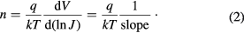
Figure 5. Dark forward J–V curve for the n-type NC-FeSi2/p-type Si heterojunctions fabricated utilizing PLD. The inset is the relationship between logJ and logV.
Download figure:
Standard image High-resolution imageFundamentally, the predominant transportation mechanism of the carriers is a diffusion process if the value of n is n = 1, while the predominant transportation mechanism is a carrier recombination process if the n value is >1 and ⩽ 2. If the n value is > 2, the predominant transportation mechanism of carrier is a tunneling process.
From the computation by using equation (2), the n value was 1.73. The implication is that the predominant transportation mechanism at the heterojunction interface between the NC-FeSi2 and Si was a carrier recombination process. The existing defects in NC-FeSi2 thin films might generate the deep energy levels in the bandgap. These energy levels could act as a center for recombination.
In the range of V > 0.2 V, the V value was sufficient to provide the carriers with sufficient energy to overcome the potential barrier at the junction. Thus, the concentration of the charge was insignificant when compared to that of the injected charges. This shows that space-charge recombination takes place and controls the transportation of the carrier [24]. In essence, if the SCLC process dominates the transportation of the carrier, the J value displays a power-law dependence of the V value as follows: J  Vm. Here, the parameter m was higher than 2. The inset in figure 5 is a plot of logJ − logV for the heterojunctions. This plot shows a linear fit between logJ and logV in the range of V > 0.2 V. The parameter m computed from the slope of straight line was 2.32. The value of m > 2 suggests that the transportation of carrier was governed by the SCLC in this bias voltage range [25, 26].
Figure 6(a) displays the C–V–f curves for the heterojunctions. The measurements performed at room temperature in the f value range of 50 kHz–2 MHz showed from the curves, that the C value decreased when the f value was increased. The G–V–f curves for the heterojunctions are displayed in figure 6(b). It was clear that the G value increased when the f value was increased.

Figure 6. (a) C–V–f and (b) G–V–f curves for the n-type NC-FeSi2/p-type Si heterojunctions in the f values range of 50 kHz–2 MHz.
Download figure:
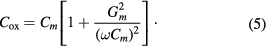
Standard image High-resolution imageThe Rs and Nss values are vital parameters for the electrical characteristics of the heterojunctions. The Nicollian–Brews method is appropriate to compute the Rs value and expressed as [27–29]:
Here, the Gm and Cm values are the conductance and capacitance in strong accumulation region, respectively, and  is angular frequency.
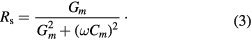
The Hill–Coleman method was employed to compute the Nss value. According to this method, the value of Nss was computed from the measured C–V–f and G–V–f curves by utilizing the following relationship [28, 29]:
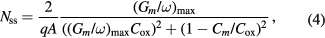
where (Gm/ω)max and Cm are the conductance and capacitance corresponding to the maximum values, A is the heterojunction area, and Cox is the insulator oxide layer capacitance and can be expressed as:
The Rs–V–f curves for the heterojunctions are displayed in figure 7. It was found that the Rs value decreased when the f value was increased. This is likely because the charges at the interface states could not follow the ac signal when the f value was high [27–29]. The Nss–f curves for the heterojunctions are illustrated in figure 8. From computation by using equation (4), the Nss values were 3.15 × 10¹⁴ eV−1 cm−2 at 50 kHz and 9.19 × 10¹² eV−1 cm−2 at 2 MHz. This proved the existence of interface states at the heterojunction interface between NC-FeSi2 and Si. These interface states acted as the center of leakage current and trap center for photo-generated carriers and thus degraded the electrical properties of the heterojunctions. In addition, it was observed that the value of Nss decreased exponentially when the f value was increased. In the region of the low f values ( f ⩽ 300 kHz), the value of Nss strongly depended on the f value, causing increasing of the C value in the n-type NC-FeSi2/p-type Si heterojunctions. The high C values at low f values were likely owing to the excess C value resulting from the Nss, which was in equilibrium with the semiconductor following the ac signal [30–32]. In contrast, the value of Nss was almost independent of the f value at f > 300 kHz. Normally, the interface states are in equilibrium with the semiconductor and do not contribute to the C value at sufficiently high f values because the charge at the interface states cannot follow the ac signal [32].
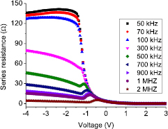
Figure 7. Rs–V–f curves for n-type NC-FeSi2/p-type Si heterojunctions fabricated by utilizing PLD.
Download figure:
Standard image High-resolution image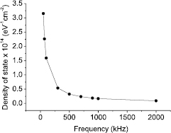
Figure 8. Nss–f curves for the n-type NC-FeSi2/p-type Si heterojunctions fabricated by utilizing PLD.
Download figure:
Standard image High-resolution image
Additionally, the carrier density for the grown NC-FeSi2 thin films utilizing PLD is approximately 1019 cm−3. This large carrier density value is expected to degrade the light detection of the fabricated n-type NC-FeSi2/p-type Si heterojunctions due to narrowing of the depletion region that expands into the NC-FeSi2 layer. Hence, the large carrier density of the grown NC-FeSi2 thin films should be further suppressed.
4. Conclusions
n-Type NC-FeSi2/p-type Si heterojunctions were fabricated by utilizing PLD at room temperature. The fabricated heterojunctions demonstrated a large reverse leakage current as well as a small NIR light response. According to the analysis of the dark forward J–V curves, a recombination process was governed at V ⩽ 0.2 V, while a SCLC process was governed at V > 0.2 V. From the computation of the Nss values by utilizing the Hill-Coleman method, the Nss values were 3.15 × 10¹⁴ eV−1 cm−2 at 50 kHz and 9.19 × 10¹² eV−1 cm−2 at 2 MHz. This proved the existence of interface states at the heterojunction interface between NC-FeSi2 and Si. These interface states acted as the center for leakage current as well as a trap center for photo-generated carriers, which was the likely cause for the degraded electrical performance of the heterojunctions at room temperature.
Acknowledgments
The present research was supported financially by a research fund of AUN/SEED-Net in the Collaborative Research Program for Alumni Members Project for Japanese Fiscal Year 2016 and King Mongkut's Institute of Technology Ladkrabang.
Footnotes
- *
Invited talk at 5th Thailand International Nanotechnology Conference (Nano Thailand-2016), 27–29 November 2016, Nakhon Ratchasima, Thailand.