
Abstract
Oblique angle deposition (OAD) is a sophisticated technique to fabricate engineered nanostructured thin films for next generation optical nanodevices. In this technique, oblique angle deposition and substrate rotation are employed to control the columnar and helical nanostructures of thin films. The films deposited by this technique show the optical anisotropy, the porosity, or the chirality, depending on the controlled morphologies at the nano-scale. In this review paper, the nanostructured optical thin film devices, such as a circular polarization handedness inverter, a linear polarization-discriminatory inverter and the selective coatings on nanopatterns, are fabricated by electron beam evaporation using the OAD technique, and their optical and structural properties as nanooptical devices are described.
Export citation and abstract BibTeX RIS

Content from this work may be used under the terms of the Creative Commons Attribution-NonCommercial-ShareAlike 3.0 licence. Any further distribution of this work must maintain attribution to the author(s) and the title of the work, journal citation and DOI.
1. Introduction
Oblique angle deposition (OAD) is a widely used physical evaporation technique to grow nanostructured porous, sculptured thin films (STFs) [1–7]. A wide variety of nanostructures, such as inclined columns, helices and zigzag shapes, can be tailored by using the OAD technique [8–10]. The sculptured thin films fabricated by the OAD technique show the optical anisotropy originating from the nanostructure and the lower refractive index than dense materials due to the nanoporous nature of the material. The high porosity and anisotropic growth behavior are caused by the self-shadowing effect and limited adatom diffusion. The degree of the anisotropy and the porosity is strongly dependent on deposition angle, material and deposition conditions. The optical anisotropy and the porosity of the thin films has various applications, such as optical retardation plates, circular polarization filters, wideband antireflection coatings, broadband high reflectors, three-dimensional photonic crystals, photonics and biomedical devices, microsensors, replication of patterns, negative index metamaterials and multiple surface-plasmon-polariton waves [11–21].
Sculptured thin films fall into two canonical classes [7]. One class of STF, the so-called sculptured nematic thin films (SNTFs), is characterized by zigzag, chevron, S-shape and C-shape columns. SNTFs have widely been used in optics as polarizers, retarders and filters. The other class, the so-called chiral STFs, is characterized by helicoidal columns, such as thin-film helicoidal bianisotropic mediums. The chiral STF reveals the circular Bragg phenomenon, i.e. it preferentially reflects circularly polarized light of the same handedness, while transmitting circularly polarized light of opposite handedness.
A multilayer STF is a cascade of single-layer STFs which are a unidirectionally non-homogeneous continuum with direction-dependent properties. The application of STFs should be extended to a wider area if various morphologies are integrated on a single substrate. For example, some properties of the SNTFs and the chiral STFs suggest that a combination of them may lead to the fabrication of various integrated optical thin film components or devices. This feasibility has motivated the study of multilayer nanostructure sculptured thin films.
The theoretical simulation for optical properties of the nanostructure sculptured thin film devices, composed of a single-layer STF as well as a multilayer STF, are studied based on the basic theory of the STFs [7]. A nanocolumnar zigzag structure reveals birefringence due to the structural anisotropy. The phase retardation depends on the birefringence and the thickness of the nanocolumnar film. A circular polarization filter of a single-section chiral STF exhibits a circular Bragg phenomenon due to periodic non-homogeneity along the thickness direction. The peak wavelength and the bandwidth in the Bragg regime strongly depend on the pitch thickness and the dielectric parameters of the circular polarization filter.
In this review paper, the morphologies of the SNTFs and chiral STFs are combined to fabricate a circular polarization handedness inverter [22], a linear polarization-discriminatory inverter [23], and selective coatings on nanopatterns, of a multilayer STF, and their optical and structural properties are described.
2. Oblique angle deposition
A schematic diagram of the OAD technique is given in figure 1(a). OAD produces directional columnar structures through the direct effect of atomic self-shadowing during film growth, while substrate rotation controls the shape of the columns. The principle of the shadowing mechanism in figure 2(b) is that as the evaporant nucleates on the substrate, the regions that become shadowed by random, agglomerated nuclei or grains do not receive any additional vapor flux. Shadowing effects lead to columnar nanostructures due to the limited adatom diffusion into shadowed areas where the boundaries or voids between columns cannot receive vapor flux. The resulting film is normally composed of approximately cylindrical columns of material, separated by voids. When the substrate is tilted such that incident vapor fluxes arrive at oblique angles, the atomic shadowing mechanism is enhanced and film growth occurs on the faces of the domed column tops facing the vapor source. As a result, the columnar nanostructure starts to become inclined toward the vapor source.
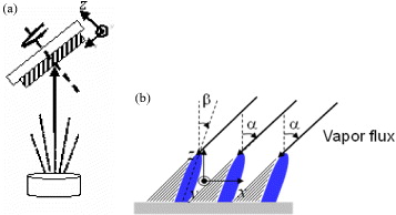
Figure 1 Schematic diagrams of (a) glancing angle deposition and (b) shadow effect.
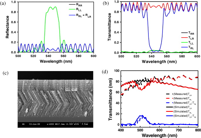
Figure 2 Circular polarization handedness inverter with zigzag and helical films. (a) Simulation of reflectance (R LR , R RR , R RL , R LL ), (b) simulation of transmittance (T LR , T RR , T RL , T LL ), (c) cross-sectional SEM images and (d) measurement and simulation of selective transmittance (T LR –T RL ) [22].
In particular, at an extremely high incidence angle, the resulting film has a highly porous nanostructure composed of isolated columns inclined toward the vapor source. Therefore the self-shadowing effect in figure 1(b) allows the production of anisotropic and porous thin films. In the OAD technique, there are three parameters that determine the morphology of the columns: the incident vapor flux angle, the substrate speed and the growth rate. By changing these parameters, a wide variety of nanoengineered morphologies can be tailored.
3. Experimental
An electron-beam evaporation with OAD technique was used to fabricate the films of zigzag and helical structures. In the experimental setup for the OAD technique in figure 1(a), high purity TiO 2 in the form of a tablet was used as an evaporation source material. The deposition was performed in a vacuum chamber with a base pressure of ∼5×10⁻⁶ Torr. The evaporation source of a 3-cm crucible pocket was located at 45 cm, directly beneath the substrate. The deposition rate and thickness of the growing films were measured by a quartz-crystal sensor, which was placed near the substrate. Glasses and polished Si (100) wafers were used as substrates for optical and structural analysis. The vapor flux incident angle, 60°, and substrate rotation speed, about 0.1 rpm, were employed to control the columnar nanostructures of the films. The deposition rate of the films was kept at 0.5 nm s −1 by using a quartz-crystal sensor. The cross-section of the OAD films was investigated using a scanning electron microscope.
4. Results and discussion
4.1. Circular polarization handedness inverter
Chiral STFs consist of helicoidal nanowires oriented perpendicular to the surface of the substrate. A helical film exhibits the circular Bragg phenomenon, i.e. it will preferentially reflect circularly polarized light of same handedness, while transmitting circularly polarized light of opposite handedness. Due to this ability to discriminate between left and right circularly polarized light, a circular polarization handedness inverter can be made of two-layer STF, a half-wave plate (HWP) with zigzag structure and a Bragg reflector with helical structure [7, 22].
An approach to solve Maxwell's equations for light propagation in a birefringent medium is known as the 4×4 matrix method, and the theory and software for STFs and chiral STFs are organized very well in a specialized book [7]. We used the software for calculation of the optical properties of STFs and chiral STFs in [7]. Figures 2(a) and (b) show the computed remittances of a circular polarization handedness inverter at ε a =2.267,ε b =2.733,ε c =2.499,χ=60°, Ω=175 nm, N=30, h=−1 and θ=ψ=0°.
Within the Bragg regime, the reflectance R LL and the transmittance T LR are very high, whereas the three reflectances, R LR , R RR and R RL , as well as the three transmittances, T RR , T LL and T RL , are very small. The subscript LR in T LR indicates left-circular polarized (LCP) light transmitted when the incident is right-circular polarized (RCP) light; and the other three transmittances are similarly defined. From these results, it is clear that the incident RCP plane wave is first transmitted through the right-handed chiral STF layer and is then inverted by the half-wave plate of the SNTF layer. Thus, this configuration acts as a circular polarization handedness inverter. Since the chiral layer is structurally left-handed, thus the incident LCP plane wave is first transformed into a RCP plane wave by the half-wave SNTF layer and is then transmitted through this left-handed chiral STF layer. In other words, the configuration acts as a circular polarization handedness inverter.
The scanning electron micrograph of an as-deposited circular polarization handedness inverter realized by a half-wave plate at 532 nm with a zigzag structure and Bragg reflector with helical structure is shown in figure 2(c). The left-handed helical structure on the top of the zigzag structure indicates the Bragg reflector with 1.5 μm thickness of 5 turns and the bottom part of the zigzag structure is the half-wave plate with 3.5 μm thickness. It is clear that the zigzag structure is oblique to the substrate while the center axis of the helical structure is normal to the substrate.
Figure 2(d) illustrates the measured and simulated transmittance spectra of the circular polarization handedness inverter. The transmittance of RCP light is higher than that of LCP light for a small range around of 523 nm. The left-handed structure of the circular polarization handedness inverter reflects the incident LCP light while transmitting the RCP light. When the RCP light is passed through the half-wave plate, it becomes LCP light on output.
4.2. Linear polarization-discriminatory inverter
A linear polarization-discriminatory state inverter made of a three-layer sculpture thin film was fabricated by the OAD technique [23]. The first and third layers of the linear polarization-discriminatory state inverter are zigzag structures that serve approximately as quarter-wave plates (QWPs), and the middle layer of them is a circular Bragg reflector of left-handed helical structure that transmits right circularly polarized light but reflects left circularly polarized light in the narrow wavelength regime.
Figure 3(a) presents the computed transmittance of the three-layer linear polarization-discriminatory state inverter at ε a =2.72,ε b =4.0,ε c =2.75,χ=60°, h=−1,Ω= 160 nm, N=20 and θ=ψ=0°. It is clear that the transmittances T SS , T PP and T PS are very small in the Bragg regime, whereas the transmittance T SP is very high. The subscript SP in T SP indicates S-polarized light transmitted when the incident is P-polarized light; and the other three transmittances are similarly defined. The maximum value of T SS is about 17% for the circular polarization filter of 20 pitches, indicating that a small portion of incident S-wave is transmitted through this device. The estimated Bragg regime of bandwidth 19.6 nm and centered at 540 nm. The trough in the spectrum of T PS and the peak of T SS increases as the number of pitches increase. The higher value of the transmittance T SP on output means that the incident linear P-polarized plane wave is first converted to the RCP plane wave by the quarter-wave plate of SNTF layer, which is transmitted through the circular polarization filter of the right-handed chiral STF layer easily and is then converted again to the linear S-polarized plane wave on output by the next quarter-wave plate of the SNTF layer. Thus, this three-layer STF device acts as a linear polarization-discriminatory state inverter.
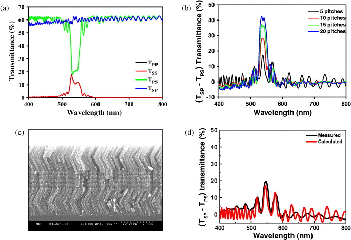
Figure 3 Linear polarization-discriminatory state inverter of a three-layer structure. (a) Simulation of transmittance (T SS , T PP , T SP , T PS ) at different pitch numbers, (b) simulation of selective transmittance (T SP –T PS ) at different pitch numbers, (c) SEM cross-section image and (d) measured and simulated selective transmittance (T SP –T PS ) [23].
So the selective transmittances (T SP –T PS ) at different pitch numbers of the circular polarization are calculated, as shown in figure 3(b). With increase in pitch number, the selective transmittance increases. The selective transmittance for the pitch number of 5 is approximately 18% and that for the pitch number of 20 is about 43%. Therefore, the inversion of the incident P-polarized light to S-polarized is more than the inversion of the incident S-polarized light to P-polarized light, indicating the conformation of a linear polarization-discriminatory state inverter.
In figure 3(c), the cross-sectional SEM image ensures the structures and positions of the QWPs as well as the Bragg reflector in the linear polarization-discriminatory state inverter, i.e. [air|QWP-Bragg reflector-QWP|glass]. The total thickness of each QWP is 2 μm and that of the Bragg reflector is 1.6 μm with 5 left-handed structural periods.
The selective transmittance (T SP –T PS ) at 545 nm in figure 3(d) is approximately 20%. These results show that the inversion of the incident P-polarized light to S-polarized light is more than the inversion of the incident S-polarized light to P-polarized light, indicating the conformation of a linear polarization-discriminatory state inverter. It is seen that the experimental results show good agreement with the simulation, but not exactly. One contributing reason is the dielectric absorption as well as dispersion effects, and another relates to index matching on either side of the fabricated device. These are not considered in our simulation. The calculated selective transmittance (T SP –T PS ) is also approximately 20% at a wavelength of 545 nm. It is clear that the top QWP layer converts the incident S-polarized light on it into a LCP plane wave, which is reflected by the left-handed Bragg reflector layer. On the other hand, incident P-polarized light is first transformed into a RCP plane wave by the top QWP, and is then transmitted easily through the left-handed Bragg reflector layer. This transmitted RCP plane wave is again converted into S-polarized light by the bottom QWP.
4.3. Selective coatings on nanopatterns
If a patterned substrate is used, the shadow effect will be enhanced greately. Figure 4 is a schematic diagram of single- and three-layer STF structures on patterned substrates, i.e. helical, zigzag and zig-helical-zag structures. Figure 5(a) is a nanopatterned photoresist (PR) on a Si substrate: the line and space of PR are 50 and 30 nm, respectively, and the height is 80 nm. Figure 5(b) shows OAD TiO 2 helical structures. The figure shows that the helical structures are on top of nanopatterns: the width of the helical structure is wider than the linewidth 50 nm of the PR and the space is narrower than that of the PR. Figure 5(c) shows OAD TiO 2 columnar zigzag structures on top of nanopatterns: the linewidth of the column is near 50 nm and the space between columns is clear. Figure 5(d) shows OAD TiO 2 zig-helical-zag structures on top of nanopatterns: the columnar zig is tilted about 40° with respect to the normal of the substrate, the helical structure grows upright on top of the columnar zig, and the columnar zag grows on top of the helical structure. These results suggest that the selective coatings on nanopatterns can be used as a way of replicating patterns [19], maskless lithography and fabrication of nanostructure metamaterials.
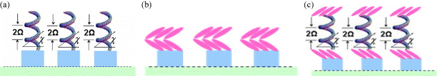
Figure 4 Schematic diagrams of STFs on patterned substrates: (a) helical structure, (b) zig-zag structure and (c) zig-helical-zag structure.
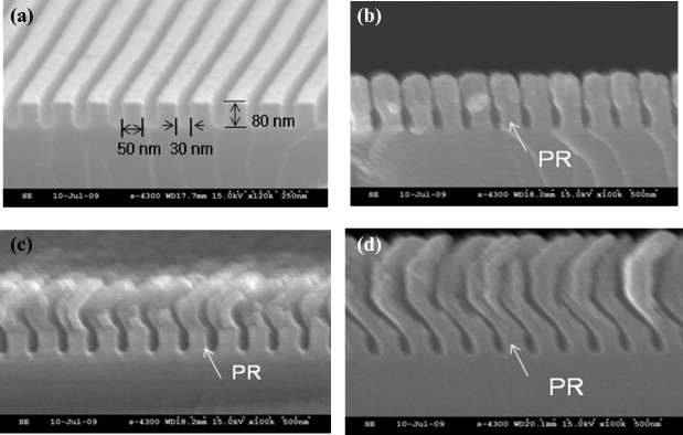
Figure 5 SEM cross-section images of OAD STF structures on patterned substrates. (a) Nanopatterned photoresist substrate, (b) helical structure, (c) zig-zag structure and (d) zig-helical-zag structure.
5. Conclusion
In this review paper, a circular polarization-discriminatory handedness inverter of a two-layer STF and a linear polarization-discriminatory state inverter of a three-layer STF are demonstrated successfully by using the OAD technique and the combination of a helical structure with a columnar zigzag structure. Also, the selective coatings on nanopatterns which enhance the shadow effects indicate that the OAD can be used as a method for replicating the patterns on a substrate, maskless lithography, and the fabrication of nanostructure metamaterials. Therefore, nanostructure engineering of optical thin films by using the OAD technique offers a possibility for the fabrication of various new optical thin film devices on a chip.
Acknowledgments
This work was supported in part by the Basic Science Research Program through the National Research Foundation of Korea (NRF) grant funded by the Ministry of Education, Science and Technology (2010–0024708), the Korea Industrial Technology Foundation (KOTEF) through the Human Resource Training Project for Strategic Technology grant funded by the Ministry of Knowledge Economy and the Dual Use Technology Program (Project No. 08-it-mc-01).