

Abstract
The coupling of electromagnetic waves with subwavelength metal structures results in the perfect light absorption and has been extensively explored in the recent years for many possible applications like photovoltaics, sensing, photodetectors, emitters and camouflaging systems to name a few. Herein we present the design and fabrication of a broadband plasmonic light absorber using aluminum as functional material for operation in the visible frequency range. The metal structures can be tuned in size to manipulate the plasmonic resonance; thereby light absorption at any desired wavelengths could be realized. Thus the broadband light absorber in the visible spectrum is designed using metal structures of different sizes supporting non-overlapping individual resonances at regular intervals of wavelengths. The metal structures of different sizes are grouped in to a single unit cell and the absorber is fabricated by periodically arranging these unit cells in a square lattice. Light absorption of more than 90% for over a broad wavelength range of 200 nm from 425 nm to 650 nm in the visible spectrum is demonstrated.
Export citation and abstract BibTeX RIS

Original content from this work may be used under the terms of the Creative Commons Attribution 3.0 licence. Any further distribution of this work must maintain attribution to the author(s) and the title of the work, journal citation and DOI.
1. Introduction
Like filtering and switching, preferential light absorption also has great importance in manipulating the flow of light in the nanoscale. Subwavelength metal structures supporting localized surface plasmon resonances (LSPR) have been actively studied as a promising candidate for the realization of perfect light absorbers in specific frequency regions [1–4]. A plethora of sensing devices has been demonstrated using different kinds of plasmonic structures both in the transmission and reflection modes [5–8]. Recently absorption engineering in plasmonic structures has been used for full colour image printing applications with resolution reaching to diffraction limit [9–14]. Another area of growing interest is in the solar photovoltaics, where plasmonic absorbers are reported to be employed for improving the energy conversion efficiency [15–18]. Sun has become the prime source of green energy and globally there is a surge in bringing down the cost of existing solar cell technology without compromising too much on the performance requirements. Recently, thin film solar cell technology based on amorphous silicon (a-Si) has emerged as an alternative to the crystalline silicon based solar cell technology in terms of cost and organic solar cell technology in terms of relatively higher theoretical conversion efficiency of about 25% [19]. Here the challenge is to meet the tradeoff between the requirements of higher optical thickness for complete light absorption and lower carrier diffusion length to minimize the unwanted carrier recombination. Hence the importance of thin light trapping surface coatings, which enhance the light absorption in to the active layer. Plasmonics has been extensively explored for the construction of thin light trapping layers in the solar cell technologies owing to their large absorption and scattering cross-sections. A recent review by Tran et al details various light trapping and plasmonic enhancement strategies in different types of solar cells reported in the contemporary literatures [20]. So far in all the reported plasmonic solar cell designs, either near field enhancement due to LSPR or forward and backward Mie scattering from embedded nanoparticles in the active layer has been employed as light trapping strategies [21]. In such designs the requirements for multiple layers consisting of antireflection coatings, active layer embedded with plasmonic nanoparticles and back reflectors lead to the poor enhancement factors, in addition to the increased system complexity which makes the practical implementation difficult.
In this paper we present the design of a broadband plasmonic light absorber, which reflects only less than 10% of the incident light indicating more than 90% light absorption in to the active layer, suitable for application in the a-Si based thin film solar cell technologies. Therefore the same broadband light absorber acts as an antireflection coating negating the requirement for additional multilayer antireflection coatings which facilitates the manufacturability and hence reduces the complexity and cost. This significantly improves overall system performance and energy conversion efficiency of the solar cells. The proposed absorber is designed in such a way that maximum amount of light is made channeled to the silicon active layer leaving near zero reflection for the entire visible region. We employed aluminum as the functional material for the realization of broadband absorber mainly due to its relatively high plasma frequency that facilitates resonant light absorption in the violet–blue region that is not possible with gold. Also low cost and abundance of aluminum makes it the widely used material in the industrial processes. Besides, aluminum facilitates the lossy interband transition outside visible spectrum, which is crucial for operation across the visible region. Apart from that, when compared with gold, aluminum does not require an adhesion layer and with silver, it does not require a capping layer, which considerably eases the fabrication processes and also brings down the cost considerably [22–24]. The design, fabrication, working principle and optical measurement followed by the discussion of results are detailed in the coming sections of this paper.
2. Design principle
Light transmission was observed in thin metal films with subwavelength hole arrays and is termed as extraordinary optical transmission (EOT) [25]. We adopted the design principle which is based on the findings by Wen et al that the enhancement of optical transmission through subwavelength holes in metals blocked by opaque metal disks [26]. The hovering metal disks over the nanoholes can couple light from free space to the subwavelength nanoholes enhancing the transmission, as shown in the figure 1(b).

Figure 1. (a) Simulated reflectance of a single nanostructure of D = 300 nm shows plasmonic resonance at 525 nm, and (b) the normalized electric field (i), power (ii) and Poynting vector (iii) calculated at the resonance wavelength of 525 nm. The Poynting vector plot clearly indicates the direction of power flow in to the substrate enhanced by EOT effect of the optical antenna structure.
Download figure:
Standard image High-resolution imageTherefore in addition to the near-field enhancement due to the surface plasmon resonance (SPR), the enhanced optical transmission in such devices can also contribute to increase the light absorption in to the active layer of thin film solar cells. Figure 1 illustrates the working principle of the proposed plasmonic light absorber modeled using finite difference time domain (FDTD) algorithm. We calculated the reflection spectrum of a single aluminum nanostructure of dimension D = 300 nm raised on top of a polymer nanopillar with perforated Al back reflector, and plotted in figure 1(a), which shows the resonance wavelength at 525 nm. The refractive index and the height h of the polymer nanopillar are assumed to be 1.5 and 150 nm in the simulation respectively and the thicknesses t of the metal square patch and the back reflector are assumed to be 45 nm. In order to study the physical origin of this resonance, we extracted the normalized values of electric field distribution, power distribution and Poynting vector as shown in (i)–(iii) of the figure 1(b), respectively, using the FDTD model. From these analyses we arrived at the conclusion that the elevated metal square patch acts as an optical nanoantenna, which couples the free space electromagnetic radiation to the LSPR modes of the Al nanostructure and the SPR modes of the perforated Al back reflector. The constructive interference between these two modes at resonance wavelength enhances the optical transmission through the nanohole left behind by the transparent polymer pillar, as evident from the Poynting vector plot that indicates the direction of the light channeling in to the substrate.
3. Absorber design and fabrication
The schematics of the unit cell of the proposed plasmonic light absorber and a single constituent nanostructure are shown in figures 2(a) and (b), respectively. The nanostructures forming the absorber is a quasi metal–insulator–metal (MIM) device in which the aluminum square patch is raised on top of the lithographically defined polymethylmethacylate (PMMA) nanopillars in the background of a perforated Al back reflector.

Figure 2. (a) Schematic showing the unit cell of the proposed plasmonic light absorber. The unit cell is comprised of metal square patches of different sizes supporting resonances at different wavelengths. (b) Schematic representation of a single nanostructure in which the Al square patch is raised on top of PMMA nanopillar in the background of a perforated Al back reflector.
Download figure:
Standard image High-resolution imageHere the requirement is for broadband absorption of light in the entire visible spectrum and it necessitates the superposition of non-overlapping multiple resonances at regular intervals of wavelengths within the operation window. The SPR and LSPR are sensitive functions of the geometry of the respective metal nanostructures and the resonance at any desired wavelengths can be realized by tuning the size of the nanostructures. Therefore in our broadband absorber design the unit cell is comprised of multiple nanostructures of different sizes supporting resonances at regular intervals of wavelengths spanning the entire visible spectrum as shown in figure 2(a). We employed metal square patches of sizes D = 180 nm, 240 nm, 320 nm and 400 nm in the unit cell, supporting plasmon resonances at wavelengths 370 nm, 450 nm, 550 nm and 650 nm, respectively.
The PMMA pillar height h is then optimized for maximum light absorption in to the substrate through the nanohole array using the FDTD model. We studied the light absorption efficiency (A) of the device for varying pillar height from 60 nm to 200 nm and found that a pillar height between 120 nm and 150 nm ensures maximum light absorption with this geometry as shown in figure 3.

Figure 3. The calculated light absorbance of the plasmonic nanostructures in the 2D array for varying PMMA pillar height showing more than 97% absorbance for a pillar height between 120 nm and 150 nm.
Download figure:
Standard image High-resolution imageHere the total light absorption is the sum of the light coupled to the plasmon modes of the resonators and the light transmitted through the nanohole arrays in to the silicon substrate and get absorbed. As evident in figure 3, the decreasing tendency of absorbance for a pillar height below 120 nm and above 150 nm can be attributed to the phase mismatch between the top LSPR and bottom SPR modes supported by the metal square patch and the back reflector respectively. Therefore the pillar height is crucial for the optimum performance of our device as a light absorber.
The fabrication of the proposed plasmonic light absorber is a two-stage process in which the pattern was generated using electron beam lithography (EBL) and transferred on to the 150 nm thick PMMA resist spin coated on a pristine silicon sample as shown in the process steps depicted in the figure 4(a). The lithography process defines the 2D arrays of PMMA nanopillars. The design file is prepared in such a way that the gap between the pillars will be exposed during the lithography process, hence can reduce the writing time considerably using the positive tone PMMA resist. Followed to the resist development and pattern transfer, an Al thin film of thickness t = 45 nm was thermally evaporated on to the sample with the patterned nanopillars, which forms both the metal square patch supporting LSPR on top of the PMMA nanopillars and the perforated back reflector supporting SPR.
The thermal evaporation was carried out at a high vacuum level of 5 × 10⁻⁶ Pa to reduce the roughness of the thin film, which in turn will reduce the scattering loss. We have captured the optical images of the sample after each step using a bright field optical microscope and the top views are shown in the figure 4(b).
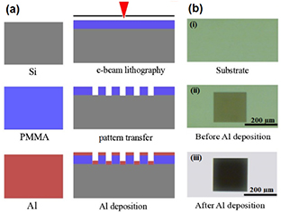
Figure 4. (a) The cross-sectional schematics of the fabrication process steps involving EBL followed by thermal evaporation and (b) top view of the sample after each step captured using a bright field optical microscope.
Download figure:
Standard image High-resolution imageThe 200 square micron area of nano pillar arrays defined by EBL depicted in the figure 4(b(ii)) with light colour displays thick black colour after the deposition of aluminum thin film, which is as shown in the figure 4(b(iii)). Therefore the colour change from grey scale to the pure black indicates the excitation of plasmon resonances and it transforms the 2D arrays of PMMA pillars in to the broadband light absorber.
The SEM image of the absorber device is shown in the figure 5 in which the unit cells are arranged in a square lattice and the magnified image of a single unit cell is shown in the inset.

Figure 5. The SEM image of the fabricated broadband absorber, inset showing the enlarged image of a unit cell consisting plasmonic structures of varying sizes.
Download figure:
Standard image High-resolution image4. Measurement and discussion
The schematic of the experimental test set up is shown in the figure 6(a) in which the light was focused normally on to the sample using an objective lens of magnification ×20 and a numerical aperture (NA) of 0.4. The same obiective was used to collect light from the sample, which is then directed to the detector using a beam splitter arragements. Therefore in the experiment, the incident light is the weighted average of many angles of excitation possible with the high NA objective lens. We have studied the spectral dependence on the incident angle using the FDTD model.

Figure 6. (a) The schematic of the experimental test set up showing high NA objective lens used for focusing light on to the sample and collecting and (b) the estimated absorbance as a function of incident angle which varied from 0° to 50°.
Download figure:
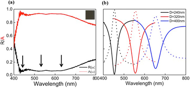
Standard image High-resolution imageIn the theoretical analysis the incident angle was varied from 0° to 50° with an increment of 5°. The estimated absorbance is plotted as a function of incident angle in the figure 6(b). It can be seen that the plasmon resonance and hence the absorbance are invariant for varying angles of incidence. The absorption band starts to broaden above an incident angle of 20° and it is also found the emergence of additional peaks above an angle of 45° in the 400–500 nm wavelength range, which can be attributed to the grating assisted excitation of surface plasmons at the aluminum-PMMA interfaces for oblique incidence [14]. The experimental reflectance R(ω) of the nano structures in their 2D array is captured using micro spectroscopic technique in the 400–800 nm wavelength range and is plotted as black line in the figure 7(a).
Figure 7. (a) Experimental reflection (black line) and absorption (red line) spectra of the fabricated structures in the 2D array (inset shows the optical image of the 2D array structure after aluminum deposition), and (b) simulated reflection spectra of individual metal structures of different sizes which forms the unit cell.
Download figure:
Standard image High-resolution image
The light was focused normally onto the sample using an objective lens of magnification ×20 and the same objective was used to collect light from the sample. The optical image captured by a CCD camera is also shown in the inset of figure 7(a). The perception of black colour is the indication of broadband near zero reflection or broadband perfect light absorption for the entire visible region. The absorbance of the structure is then calculated using the equation ![$A\left( \omega \right)=1-\left[ T(\omega)+R(\omega) \right]$](https://content.cld.iop.org/journals/2043-6262/9/1/015010/revision1/ansnaaabb0ieqn001.gif) and is plotted as red line in the figure 7(a), where the experimental transmittance T(ω) is zero due to the opaque silicon substrate and hence the A(ω) represents the amount of light absorbed by the silicon substrate, which is enhanced by the plasmonic effect discussed in section 2 of this manuscript. The black arrows in the figure 7(a) represent the positions of individual resonances, which are separately simulated and shown in the figure 7(b) in which the solid lines represent the reflectance and the dotted lines represent the corresponding absorbance. The nanostructure of size D = 180 nm has plasmonic resonance slightly above blue and it was included in the unit cell for filling the gap when it is periodically arranged in the 2D arrays.
and is plotted as red line in the figure 7(a), where the experimental transmittance T(ω) is zero due to the opaque silicon substrate and hence the A(ω) represents the amount of light absorbed by the silicon substrate, which is enhanced by the plasmonic effect discussed in section 2 of this manuscript. The black arrows in the figure 7(a) represent the positions of individual resonances, which are separately simulated and shown in the figure 7(b) in which the solid lines represent the reflectance and the dotted lines represent the corresponding absorbance. The nanostructure of size D = 180 nm has plasmonic resonance slightly above blue and it was included in the unit cell for filling the gap when it is periodically arranged in the 2D arrays.
It is to be noted that the non-overlapping resonances superposed together to form the broadband absorption of more than 90% obtained in figure 7(a). As apparent in experiment and simulation, the decreasing tendency of absorbance for wavelengths beyond 650 nm is due to the presence of lossy interband transition of aluminum at a wavelength around 800 nm. A flat reflection valley of over 200 nm in the 425–650 nm wavelength range with less than 10% intensity is achieved with this design strategy. Therefore the simple design combined with the comparable performance with other designs make our broadband absorber suitable for application in the thin film a-Si solar cell technology.
5. Conclusion
We have demonstrated the design and fabrication of a broadband light absorber in the visible region of electromagnetic spectrum for possible applications in the solar cell technology. A flat reflection valley of less than 10% intensity over a broad spectrum of 200 nm from 425 nm to 650 nm is achieved, which indicates more than 90% light absorption in the entire visible spectrum. Inexpensive aluminum is used as the functional material, which facilitates the resonant absorption in the violet–blue region widening the useful spectrum for solar conversion. Also Al is CMOS compatible and a widely used material in the industrial processes, furthering the applicability of our plasmonic light absorption strategy.
Acknowledgments
This work was supported by the foreign postdoctoral research fellowship provided by RIKEN. The work made use of the RIKEN's nano fabrication facility in the emergence matter science department and simulation and characterization facilities in Metamaterials laboratory. This work was also partially supported by Innovative Science and Technology Initiative for Security, ATLA, Japan.