


Abstract
In this paper, the impact of process variation on the performance parameters of junctionless silicon nanotube field effect transistor (JLSiNT-FET) is studied using 3D numerical simulations. The performance metrics, ON current, OFF current, and unity gain frequency are taken for different physical factors. Sensitivity of the physical factors is computed over a range at various points. The ranking of the structural parameters for various performance metrics is done using a two level full factorial design of experiment method. Overall ranking proposes that the outer diameter of the silicon tube is the most sensitive parameter and inner diameter of the silicon tube is the least sensitive parameter.
Export citation and abstract BibTeX RIS

Original content from this work may be used under the terms of the Creative Commons Attribution 3.0 licence. Any further distribution of this work must maintain attribution to the author(s) and the title of the work, journal citation and DOI.
1. Introduction
Conventional single gate planar MOSFET has evolved into multi-gate devices such as FinFETs to deal with the short channel effects [1, 2]. Silicon nanotube field effect transistor (SiNT-FET) is known as the advanced version of the multi-gate structures that was explored in 2012 [3]. Since SiNT-FET has the tubular channel controlled by the inner and outer gates, it gives enhanced performance in terms of excellent channel control compared to the silicon nanowire (SiNW) structure [4]. The tunneling operation is realized on SiNT-FET structure in reference [5]. Junction-less operation is realized on the SiNT-FET structure (JLSiNT-FET) in the literature [6] since junction-less transistor has been appeared as one of the most expectant device due to their better immunity to short channel effects (SCEs) and well-matched process flow with the existing CMOS technologies [7].
In the device manufacturing, the process induced variations are inevitable. There have been many literatures available for process variations on MOSFETs and FinFETs [8–11]. Literatures [12, 13] discuss about the sensitivity of the gate-all-around (GAA) MOSFETs to process variations. Analysis of scalability and process variation on SiNW was explored in [14–16]. Process variation study on the vertical SiNW tunnelling FET was done in [15]. Since the SiNT-FET has excellent scalability over SiNW, the impact of the process variation on conventional junction based SiNT-FET is done in [17]. The tube wall thickness and gate length dependencies on the output parameters of JLSiNT-FET are presented in reference [6]. The important physical parameters, silicon tube ovality and gate oxide thickness also influence the characteristics of the device apart from silicon wall thickness and gate length, and hence an organized study of structural process variation together with the important factors such as, silicon tube ovality, gate oxide thickness for inner and outer gates of JLSiNT-FET is to be studied.
In this paper, we have realized the impact of process variation on six important structural factors such as gate length  , outer gate oxide thickness
  , inner gate oxide thickness
  , silicon tube wall thickness for two cases: (i) for constant outer diameter (OD) and (ii) for constant inner diameter (ID), and silicon tube ovality. The performance metrics such as ON current
  , OFF current
  , Threshold voltage
  and unity gain cut-off frequency
  are provided. The ranking of the structural factors is done using two level full factorial design of experiments (DOE) method.
The rest of the paper is organized as follows. The device description and calibration are dealt in section 2. Section 3 discusses the sensitivity analysis over a range for different structural factors. The ranking of the structural parameters is done using DOE method in section 4. Finally, conclusions are given in section 5.
2. Device structure and  calibration

To execute the simulations, Sentaurus Structure Editor and Sentaurus Device Simulator from TCAD are used. To do the device simulations, Drift-diffusion transport model is used. Normal field degradation, high field saturation, degradation due to doping, degradation due to interface are taken care in the simulations. Carrier carrier scattering, Doping Dependency model, Philips Unified Mobility model and Lombardi models at interface are included in the simulations. Considering the smaller dimensions of the device, Quantum corrections are also included [18]. Based on ITRS standard for the given technology, 50 Ω resistor is added with source and drain contacts in the electrode section of the simulator during AC analysis.
The device structure and its current-voltage characteristics from [6] are used for the device calibration. JLSiNT-FET device created by TCAD is given in figure 1(a), showing all the regions of the device. JLSiNT-FET with gate oxide and spacer removed i.e. Silicon portion alone is shown in figure 1(b). The schematic vertical cross section of the JLSiNT-FET is given in figure 1(c). The schematic circular cross section of the JLSiNT-FET is given in figure 1(d). JLSiNT-FET device details are given in table 1. The calibrated ID–VG characteristics plot is given in figure 2.
Table 1. Device details of JLSiNT-FET.
| S. No. | Parameters | Dimensions |
|---|---|---|
| 1 | Gate length | 45 nm |
| 2 | Tube wall thickness | 5 nm |
| 3 | Tube outer diameter | 32 nm |
| 4 | Tube inner diameter | 22 nm |
| 5 | Oxide thickness | 1 nm |
| 6 | Drain/source length | 15 nm |
| 7 | Drain/source wall thickness | 15 nm |
| 8 | Spacer length | 25 nm |
| 9 | Doping concentration |  |
| 10 | Gate electrode work function | 4.68 eV |

Figure 1. (a) JLSiNT-FET structure showing all the regions; (b) silicon portion alone of JLSiNT-FET structure; (c) schematic vertical cross section of JLSiNT-FET; (d) schematic circular cross section of JLSiNT-FET.
Download figure:
Standard image High-resolution image
Figure 2.  characteristics of SiNT-FET calibrated against the published result in [6].
Download figure:
Standard image High-resolution image3. JLSiNT-FET structural factors sensitivity analysis
The structural parameters of JLSiNT-FET such as  ,
,  ,
,  ,
,  and silicon tube ovality
  are varied over a range. Using the sensitivity analysis, these above structural parameters impact on
  and unity gain frequency
  are studied. As already stated in introduction, the
  can be changed either by changing OD (ID constant), or by changing the ID (OD constant) of the silicon tube.
Sensitivity analysis has been done for one factor at a time with  variations (keeping all other parameters constant). The expression (1) given below is used to compute the sensitivity in which
  is the change in the performance metrics,
  and
and  and
and  is the change in the structural factors,
  ,
,  ,
,  ,
,  ,
,  and
and 
3.1. Structural factors impact on and


In this subsection, the impact of structural factors on  and
and  is given. Variation of
  and
and  is plotted against
  ,
,  ,
,  ,
,  , and
, and  , and are given in figures 3–8. The structural parameters values are given in table 2. Their sensitivities are also calculated in this range as given in expression (1) at various points and sensitivity as a function of
  ,
,  ,
,  ,
,  , and
, and  are plotted in the graphs (figures 3–8).
Table 2. Structural factor values of JLSiNT-FET.
| Structural factors | Nominal value | Range |
|---|---|---|
 (nm) (nm) |
45 | 18–100 |
 (nm) (nm) |
5 | 4–8 |
 (nm) (nm) |
1 | 1–2 |
 (nm) (nm) |
1 | 1–2 |
Ovality  (ratio between major to minor axis) (ratio between major to minor axis) |
1 | 1–1.75 |
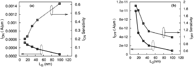
Figure 3. (a)  and its sensitivity as a function of
  ; (b)
; (b)  and its sensitivity as a function of
  .
.
Download figure:
Standard image High-resolution image
Figure 4. (a)  and its sensitivity as a function of
  ; (b)
; (b)  and its sensitivity as a function of
  .
.
Download figure:
Standard image High-resolution image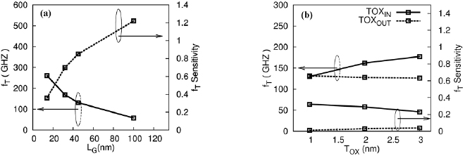
Figure 5. (a)  and its sensitivity as a function of
  ; (b)
; (b)  and its sensitivity as a function of
  .
.
Download figure:
Standard image High-resolution image
Figure 6. (a)  and its sensitivity as a function of
  ; (b)
; (b)  and its sensitivity as a function of
  .
.
Download figure:
Standard image High-resolution image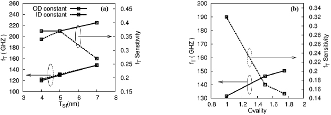
Figure 7. (a)  and its sensitivity as a function of
  ; (b)
; (b)  and its sensitivity as a function of ovality.
Download figure:
Standard image High-resolution image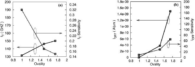
Figure 8. (a)  and its sensitivity as a function of ovality; (b)
  and its sensitivity as a function of ovality.
Download figure:
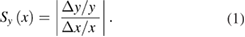
Standard image High-resolution imageAs  decreases
  is expected to increase which can be confirmed from figure 3(a) as expected. ION sensitivity is increased with respect to
  . Figure 3(b) shows the usual
  versus
  characteristics and
  sensitivity decreases with respect to
  .
.
Since JLSINT-FET has two gate oxides (inner and outer), there are two cases: (i) varying  (
( is constant) and (ii) varying
  (
( is constant). Figure 4(a) depicts that
  and its sensitivity as a function of
  . It can be observed from figure 4(a) that
  decreases when
  or
or  is increasing.
  's sensitivity is also decreased with respect to
  and
and  . The sensitivity is higher for
  and this is due to the rate of decrease in effective gate oxide thickness is more when
  is increased compared to
  [17]. The effective oxide thickness is expressed as follows:
where  ,
,  ,
,  and
and  are as shown in figure 1(d).
Figure 4(b) shows  versus
  plot along with its sensitivity. It can be observed from figure 4(b) that when
  increases, the channel control by the gates reduces, and hence,
  increases. Figure 5(a) gives
  versus
  diagram.
  decreases when
  increases. The simulation results go with the
  trend with a coefficient value
  of 0.98.
  sensitivity is increasing with respect to
  . Figure 5(b) depicts
  as a function of
  and
and  . We can see from figure 5(b) that
  increases with
  . We can see from JLSiNT-FET structure (figure 1(a)) that the inner gate is covering all drain, channel and source regions and hence the inner associated parasitic is more compared with the outer gate (outer gate of JLSiNT-FET is covering only the channel portion). When increasing the inner gate oxide thickness
  , the parasitic associated to inner gate reduces. We also know that

where,  is the trans-conductance,
  is the combination of gate to source capacitance
  , gate to drain capacitance
  , and overlap capacitance
  . When
  reduces,
  increases which can be confirmed with the figure 5(b). From figure 5(b), it can also be noted that
  is more sensitive to
  compared to
  .
.
As mentioned already, the silicon tube thickness can be changed either by changing OD (for constant ID) or by changing the ID (for constant OD). The silicon tube thickness  can be changed either by changing OD (for constant ID) or by changing the ID (for constant OD). Channel width is given as
  for outer channel and
  for inner channel where,
  and
and  . For constant ID, to increase
  the OD should be increased and hence the channel width also increases. This results the current to increase for constant ID. For constant OD, to increase
  the ID should be decreased and hence the channel width decreases. This makes the current to decrease for constant OD. The above statement is true for the absolute values of current and not true for normalized values of current. Figure 6(a) shows that
  and its sensitivity as a function of
  . From figure 6(a) it can be seen that the normalization current goes up when
  increases for both constant ID and constant OD cases.
  's sensitivity is decreased when OD is constant whereas
  's sensitivity increased when ID is constant. Figure 6(b) shows that
  and its sensitivity as a function of
  . When
  increases leakage cross section increases, and hence,
  increases which can be noted from figure 6(b).
  's sensitivity also increases with respect to
  .
.
Figure 7(a) gives the  and its sensitivity as a function of
  . It can be seen from figure 7(a) that the
  and its sensitivity increase with respect to
  for both constant ID and constant OD cases. It can be observed from figure 7(a) that for increasing the
  we need to decrease the ID (for constant OD case), results reduction in inner gate area, and hence one can anticipate the
  to reduce. But this inner gate area reduction reduces the parasitic associated with that and thereby increases
  . To increase the
  , we need to increase the OD (for constant ID case). This will increase the outer gate area, which will increase the
  and
and  but
but  takes over
  to increase.
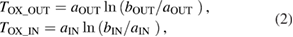
Normally Silicon tube is intended to be a circular shape but because off the critical fabrication procedures, it will end up with oval shape. To capture that effect in device characteristics, the ovality  of the silicon tube is also varied here. When ovality is 1, the perfect circular tube shape will occur otherwise the oval shape will occur. Figure 7(b) shows fT and its sensitivity as a function of
  . It can be noted from figure 7(b) that
  increases due to an increase in the channel width and small reduction in effective oxide thickness with
  . More sensitivity is observed in larger
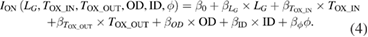
  . ION and its sensitivity as a function of
  are depicted in figure 8(a). It can be noted from figure 8(a) that when
  increases
  increases due to the channel width increases. When
  , the JLSiNT-FET is more sensitive.
  versus
  plot is shown in figure 8(b). When
  increases, the gate control on the channel reduces and so the
  increases (from figure 8(b)).
4. Ranking of JLSiNT-FET's structural factors
In this section, the structural factors ranks have been done using a two level factorial DOE method for  deviation from the nominal values (table 2). The performance parameters,
  , threshold voltage
  , sub-threshold swing (SS) and
  , are written as a first order polynomial expression, as a function of input factors,
  ,
,  ,
,  ,
,  , and
, and  . The expression (2) shows the example for
  [17]:
[17]:
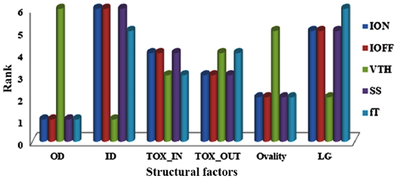
Based on the  value (coefficient terms), the ranking of structural parameters has been done. Expressions for other performance parameters can also be done similarly. Figure 9 shows the individual structural factors ranks that are computed in the above manner. It can be observed from figure 9 that the OD has occupied the first rank and ID has occupied the last rank on the impact of performance metrics, except for
  . It is observed that
  is more sensitive compared to
  in the case of
  whereas in the case of
  , it is vice versa.
Figure 9. Individual ranking for structural factors of JLSiNT-FET.
Download figure:
Standard image High-resolution image
Overall sensitivity of structural factors is calculated by adding all the β values. Adding all the β values and arranging them in the descending order, the overall ranking is evaluated and is given in table 3. One can observe that OD is the most sensitive factor and ID is the least sensitive parameter. Table 3 depicts that the OD and ovality occupy the top two ranks. The last two ranks are occupied by LG and ID.
Table 3. Overall ranking for the structural parameters of SiNT-FET.
| Rank | Structural factors |
|---|---|
| 1 | OD |
| 2 | Ovality |
| 3 |  |
| 4 |  |
| 5 |  |
| 6 | ID |
5. Conclusion
In this paper, we have examined the effect of structural factors,  ,
,  ,
,  ,
,  , and silicon tube ovality, on the performance metrics,
  ,
,  ,
,  ,
,  and
and  of JLSiNT-FET using 3D numerical simulations. The investigation is done by the three ways: (i) varying the structural factors over a range and finding their impact on each of the performance factors; (ii) calculating their sensitivity by performing
  deviations at different points over a range; and (iii) individual and overall ranking of structural factors with respect to each performance metric using DOE method. The results in the overall ranking show that the OD is the most sensitive factor whereas the ID is the least sensitive factor. Ovality is the significant factor next to OD.