


Abstract
The conditions for the synthesis of zinc, copper and iron oxides nanostructures using plasma nanosecond high-current discharge in air when introducing electrodes material vapor into a plasma due ectonic mechanism and the main parameters of the plasma are investigated. It is shown that this discharge can be used for the synthesis of nanoparticles of transition metal oxides on a dielectric substrate. Optical characteristics of nanostructures are given.
Export citation and abstract BibTeX RIS

Original content from this work may be used under the terms of the Creative Commons Attribution 3.0 licence. Any further distribution of this work must maintain attribution to the author(s) and the title of the work, journal citation and DOI.
1. Introduction
The development of nanosecond and subnanosecond high-current technology [1] led to wide applications of these devices in various fields of physics and technology [2–4]. Investigation of powerful nanosecond discharges between metal electrodes in air has shown that selective 'point' lamps on metal vapors can be developed on their basis [5, 6]. It is of practical interest to search for new applications for such discharges in highly overstressed gaps, which are accompanied by the generation of a runaway electron beam [7].
One of the promising applications of a nanosecond discharge in the atmospheric pressure air can be the synthesis of nanostructures based on metals and more complex semiconductor compounds such as chalcopyrite [8]. In the case of a nanosecond discharge in air in short discharge gaps (0.5–2 mm), the formation of ectons is observed, which is accompanied by microexplosions of natural inhomogeneities on the surface of metallic or semiconductor electrodes and the ejection of vapors of electrode material into the gaseous medium [9]. When using the air or pure oxygen in such plasma, it is possible to form metal oxides and synthesize corresponding nanostructures on their basis. The nanostructures of metal oxides are currently produced by various physical methods from the gas phase with thermal, laser and magnetron sputtering. Laser methods for the synthesis of nanostructures are valuable, require the use of qualified personnel and are characterized by a low yield of the final product, while other gas-discharge methods require the use of cost vacuum equipment.
A theoretical model for the synthesis of nanostructures in a laser and gas-discharge air plasma of atmospheric pressure, which predicted the formation of nanostructures with radii in the range of 2–10 nm with an energy contribution to the streamer discharge at the level (0.1–0.25) is considered in [10, 11] reported on the synthesis of molybdenum and titanium nanostructures in a nanosecond discharge of atmospheric pressure, which was ignited in the discharge gap  with positive pulses of amplitude (7–13) kV, duration 40 ns and frequency
  . Data on the study of the conditions for the synthesis of nanostructures based on transition metals (Cu, Zn and Fe) in overstressed nanosecond discharge in the atmospheric pressure air are not available in the literature known to us; therefore, the problem of studying the synthesis conditions and the main characteristics of such nanostructures in the atmospheric pressure air without the use of expensive laser and vacuum equipment is actual.
The results of the investigation of the spatial, electrical and optical characteristics of overstressed nanosecond discharge between electrodes from a number of transition metals (zinc, copper, iron) in air under conditions of a sufficiently homogeneous electric field strength distribution in the 'sphere-sphere' discharge gap are presented, as well as characteristics of thin nanostructured films synthesized from sputtering products of metal electrodes and components of the air nanosecond plasma discharge. The process of synthesis of nanostructures was accompanied by intense irradiation of the substrate with a nanosecond discharge plasma in the spectral range 200–300 nm, which is important for improving their electrical characteristics [12].
2. Discharge module and plasma diagnostics
The scheme of discharge chamber with a system of electrodes and a substrate for deposition of nanostructures is presented in figure 1. Electrodes for ignition of nanosecond discharge were made of zinc, copper or stainless steel. They were placed in a dielectric discharge chamber, which had a volume  . The distance between the electrodes could be adjusted within 0.001–0.005 m. The air pressure in the chamber varied in the range 6–303 kPa. The discharge chamber could be evacuated to a residual pressure 10 Pa, but most experiments were carried out at an air pressure 101 kPa [13]. The diameter of the cylindrical metal electrodes was 0.005 m and the radius of the rounding of the working end part was 0.003 m. At this ratio between the radius of the electrode rounding and the value of the interelectrode distance, the distribution of the field strength in the gap is relatively uniform [14]. To locate the discharge in the interelectrode gap, the metal electrodes were inserted into the tubes of PTFE, so that the length of their isolated parts did not exceed 0.003 m. When the dielectric tubes on nanosecond discharge electrodes are used, the discharge glow zone expands [15].

Figure 1. The structure of the gas-discharge cell: (1) is the dielectric cell housing, (2) is the substrate fastening system for deposition of thin films, (3) is the electrode spacing adjustment system, (4) is the metal electrodes, (5) is the spatial deposition zone of the films, (6) is the glass substrate for films deposition, (7) is a film based on the material of electrodes and fractions of air plasma.
Download figure:
Standard image High-resolution imageTo ignite a high-current nanosecond discharge, bipolar high-voltage pulses with a total duration 50–100 ns and an amplitude  from a power supply of ultraviolet nitrogen laser (337.1 nm) with the longitudinal low pressure glow discharge of LGI type were applied to one of the electrodes. In this case, a diffuse discharge with an amplitude of current pulses 50–170 A was ignited between the end parts of the metal electrodes of a spherical shape. The volume of the plasma did not exceed
  . When the distance between the electrodes was
  at the atmospheric pressure air, the discharge gap was overstressed, since for the non-overstressed gap in the air
  the electric field strength is 0.30 kV m−1 [16], and in these experiments it reached 3–5 kV m−1. The repetition rate of pulses varied in the range
  .
.
The voltage pulses on the discharge gap and the discharge current were measured using a broadband capacitive voltage divider, Rogowski coil, and the broadband oscillograph 6 LOR-04. The spatial characteristics of a nanosecond discharge were studied using a digital camera. To register the radiation spectra of the discharge, we used a monochromator MDR-2, a photomultiplier FEU-106, a direct current amplifier, and an electronic potentiometer. The plasma radiation was analyzed in the spectral range 200–650 nm. Measurement of the radiation power of the point lamp was performed with the help of the ultraviolet absolute radiation power meter 'TKA-PCM', which was tuned for measurement in the spectral range 200–280 nm.
The transmission spectra of thin films that were synthesized on glass substrates were recorded with the OCEAN OPTICS USB 2000 spectrometer. The radiation that probed the substrate with the film was fed to the latter using an optical fiber system.
The films were sputtered during 20–40 min when the glass substrate was installed at a distance 0.03 m from the center of the discharge at an air pressure 101 kPa, the distance between the electrodes was 0.001 m, and the amplitude of the voltage pulses was  . Analysis of the surface of the film was carried out using an electron microscope.
Photoluminescence spectra of synthesized films were investigated by irradiating a film with a high-pressure arc mercury lamp at three wavelengths: 279, 330, 380 nm. At the same time, the emission of a mercury lamp in the spectral intervals of 5 nm was standing out in the vicinity of the wavelengths 279, 330, 380 nm with a monochromator and directed to the surface of the film. The photoluminescence spectrum of the nanostructures was recorded with the help of another monochromator, equipped with a separate photoelectric radiation detection system.
The surface image of the films was recorded using a Scanning Electron Microscope CrossBeam Workstation Auriga (Carl Zeis). Raman scattering spectra were excited using an argon ion laser, which generated radiation at a wavelength of 514.5 nm. The Raman scattering spectra on the nVia Renishaw spectrometer were recorded.
3. Characteristics and parameters of discharge plasma
The radiation regime of the discharge plasma in the form of a 'point' lamp was achieved only at repetition rates of voltage pulses 0–150 Hz (figure 2).
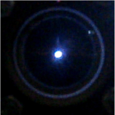
Figure 2. Images of overstressed nanosecond discharge between copper electrodes at a repetition rate 40 Hz.
Download figure:
Standard image High-resolution imageWith an increase in the repetition rate of voltage pulses to 1000 Hz, the diameter of the plasma formation grew by 3–4 times. The spherical shape of the plasma glow zone can be due to the use of dielectric tubes on the electrodes and the accumulation of low-mobility positive ions on the dielectric surface, which are formed as a result of ionization processes near the electrodes and lead to a change in the configuration of the electric field in the interelectrode gap [15].
In figure 3 the voltage oscillogram between copper electrodes in air is showed. When using electrodes made of zinc or stainless steel, the voltage oscillograms of the nanosecond discharge were close to the oscillogram shown in figure 3. Because of the mismatch of the output resistance of the high-voltage modulator with the discharge resistance and the presence of reflected pulses from the discharge gap with the plasma, the voltage pulse consisted of individual spikes with a duration of about 5–10 ns. The duration of the main part of the train of voltage pulses reached 50–100 ns. Bipolar voltage pulse spikes had the amplitude of positive and negative component up to 15–20 kV.
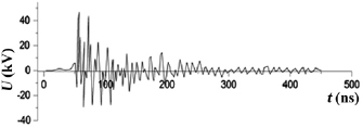
Figure 3. The voltage oscillogram on the discharge gap between copper electrodes (air pressure 101 kPa,  ).
).
Download figure:
Standard image High-resolution imageCurrent pulses of a nanosecond discharge were a sequence of bipolar current pulses with the amplitude of positive and negative components 120–150 A. The duration of the current pulse train with a time-decreasing amplitude reached 150–200 ns. The maximum pulse discharge power was observed at the initial stage of the breakdown of the discharge gap and reached 4 MW. For the conditions of ignition of a nanosecond discharge at an air pressure 101 kPa, the value of energy introduced into the plasma was 105 mJ.
Investigation of plasma radiation spectral characteristics of a high-current nanosecond discharge in atmospheric pressure air between electrodes from transition metals (Zn, Cu, Fe) has shown that about 80%–90% of its radiation power from the spectral range 200–650 nm is concentrated in spectral intervals 200–220 nm (electrodes with Zn), 200–230 nm (Cu), (200–260 nm) (200–300) nm (Fe).
In figure 4 the radiation spectrum of overstressed nanosecond discharge in air is shown. With a significant overstress of the discharge gap, when the distance between the electrodes is minimal  in the atmospheric pressure air, two groups of intense spectral lines of zinc atom and ion in the spectral range 200–280 nm are found in the plasma emission spectra. The most intense in the first group of spectral lines were ion lines: 202.6, 206.2 nm Zn II, and in the second group the spectral lines of the zinc atom are 250.2, 255.8 nm Zn I.
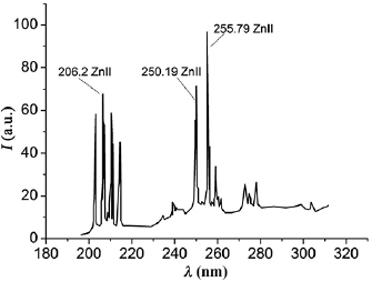
Figure 4. Plasma radiation spectrum of overstressed nanosecond discharge in air (at  ,
,  ).
).
Download figure:
Standard image High-resolution imageWhen the distance between the electrodes is increased to  at atmospheric pressure air, the electric field in the discharge gap decreases, which leads to a decrease in the electron temperature and a worsening of the conditions of x-ray preionization. At the same time, the intensity of spectral lines of zinc atoms and ions radiation from the spectral interval 200–215 nm decreases practically to zero, and the intensity of the atomic spectral lines of zinc (from the interval 250–280 nm) decreases by several times. For the air plasma with small impurities of zinc vapor at
  , the spectral lines of zinc in the wavelength intervals 250–280, 330–350, 460–510 nm become the main ones.
UV radiation spectra  of nanosecond discharge plasma in air
  between electrodes from copper are given in [17]. The UV spectrum obtained by us is well correlated with the emission range of a unipolar subnanosecond discharge with a beam of runaway electrons between copper electrodes at an interelectrode distance 0.0005 m, as well as for a unipolar nanosecond discharge of the lower power between copper electrodes in the atmospheric pressure air [5, 6]. The emission spectra are dominated by transitions from the energy states of singly charged ions 8.23–9.12 eV with a change in the electron configuration
  , as well as the spectral lines of copper atoms, which are fixed at transitions from highly excited states of the copper ion with energies in the range
  .
.
In figure 5 a region of the emission spectrum with the most intense spectral lines for the nanosecond discharge plasma between the stainless steel electrodes is presented. The interpretation of the spectrum showed that the spectral lines of atoms and singly charged iron ions dominate in the discharge between stainless steel electrodes, and the spectral line 249.6 nm FeI is the most intense. Our results correlate well with the corresponding emission spectra of a high-voltage subnanosecond discharge in the atmospheric pressure air for a system of 'needle-plane' electrodes at  , in which the running electrons play a significant role [18].
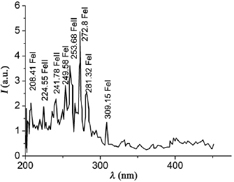
Figure 5. The radiation spectrum of nanosecond discharge plasma between stainless steel electrodes (the air pressure is 101 kPa,  ,
,  ).
).
Download figure:
Standard image High-resolution imageThe dependence of the average power of the UV radiation of a nanosecond discharge in the spectral range 200–280 nm on the frequency was nonlinear, its maximum increase was observed in the frequency range 40–350 Hz. With an increase in the repetition rate of voltage pulses from 35 to 1000 Hz, the average power of the UV radiation of the discharge grew by an order of magnitude. An increase in the charging voltage of the working capacitor from 13 to 20 kV (at  ) resulted in an increase in the power of the UV radiation of the discharge only by a factor of two. The obtained results show that to increase the average power of the UV radiation of the discharge, the most promising is an increase in the repetition rate of the voltage pulses.
Modeling of plasma parameters was carried out for a nanosecond discharge in the atmospheric pressure air between copper electrodes. Copper vapors were introduced into the plasma due to the erosion of the electrodes. As in [19], where an atmospheric air plasma with small impurities of a copper electrode vapor was investigated and where the partial pressure of copper vapor was estimated at the level of a tenth of a percent, a partial pressure of copper vapor at a level of 100 Pa was chosen for our estimates. Under the conditions of these experiments, the maximum value of the parameter  reached about
  , less than the critical value
  for nitrogen according to the local electron runaway criterion of
  [16]. Therefore, to simulate the plasma parameters of atmospheric pressure air with small admixtures of copper vapor, a standard program was chosen for the solution of the Boltzmann kinetic equation for the electron energy distribution function (EEDF) [20].
On the basis of the calculated EEDF, mean energy and mobility of the electrons were determined, the specific power losses of the discharge on various electronic processes and the rate constants of elastic and inelastic scattering of electrons by copper, argon and carbon dioxide, oxygen and nitrogen molecules, the ratio of which in atmospheric pressure air was  , depending on the magnitude of the reduced electric field (the ratio of the electric field strength E to the total concentration of copper vapor and gases which are included in the atmosphere
  ). The range of the parameter change is
  . A set of effective cross sections of electronic processes, taken into account in modeling and the main expressions for calculating plasma parameters are given in the description of the program [20].
Mean electron energy in the discharge almost linearly increases from 0.15 to 29.1 eV with the increase of the parameter  from 1 to 1300 Td. For the range of reduced electric field strength (615–820) Td, at which experimental studies of discharge characteristics were performed, mean electron energy varied within the range 12.5–16.0 eV. The electron temperature increases in the range (145000–185600) K when the parameter E/N varies from 615 to 820 Td. The value of the electron concentration is in the range
  at a current density
  on the electrode surface (
 ). The calculated electron density is well correlated with the experimentally determined maximum value of the electron density in the arc discharge between different composite electrodes (
 ) [21, 22].
The maximum specific power losses of the discharge on inelastic electronic processes in the discharge on a mixture of copper vapor with air (figure 6) were observed for the nitrogen molecule and reached 32.7% for excitation of the sum of the singlet states of the nitrogen molecule with a reduced electric field strength 820 Td (curve 2, figure 6).

Figure 6. The dependences of the specific power losses of the discharge on the processes of collisions of electrons with the nitrogen molecule on the value of the E/N parameter in the plasma on a mixture of 'copper vapor: air = 100 Pa: 101 kPa' at a total air pressure  : (1)- ionization of the nitrogen molecule by electrons, (2)- excitation of the sum of singlet states of the nitrogen molecule, (3)- excitation of the
  state, (4)- excitation of the
  state, (5)- excitation of the
  state, (6)- excitation of the
  ,
,  state, (7)–(14)- excitation:
  ,
,  ,
,  ,
,  ,
,  ,
,  ,
,  states.
Download figure:
Standard image High-resolution imageFor the copper atom, the specific power losses of the discharge reached a maximum value 2.9% to excite its  resonance state at
  . With an increase in the parameter
  up to 1300 Td, the specific power losses in the discharge reached a maximum 40.2% for the process of ionization of the nitrogen molecule by electrons. The rate constants are characterized by large values
  , which is due to the large effective cross sections of the corresponding processes. In the range of the reduced electric field strength (615–820) Td, the excitation constants of the
  ,
, 
 ,
,  states of copper and its ionization are within
  ,
,  ,
,  ,
,  and
and  , respectively.
In the range of reduced electric field strength (615–820) Td, the rate constants of excitation of the electronic states of the nitrogen molecule were in the range  . The maximum value
  was observed for the excitation of the sum of the singlet-singlet states of a nitrogen molecule with a threshold energy 13 eV for a reduced electric field strength 820 Td.
4. Optical characteristics of nanostructures
All studies of the synthesis conditions and optical characteristics of nanostructured films were carried out from the sputtering products of metal electrodes at an air pressure  and a distance between the electrodes
  . Figures 7 and 8 present images of the surfaces of the films deposited from nanosecond discharge plasma between copper and zinc electrodes in the air. To determine the size of nanostructures, a gel based on standard spherical nanostructures of gold with a diameter 20 nm was applied to the surface of the film (they are highlighted in yellow in the image, figure 7). A comparative analysis of the sizes of spherical gold nanostructures and nanostructures synthesized from nanosecond discharge products showed that the sizes of synthesized nanostructures are in the range 2–20 nm. The cross-section of zinc-based nanostructures had dimensions generally in the range of 10–50 nm, but also the formation of micron-sized zinc agglomerates was observed. Investigation of the surface of the cross-section of nanostructures and a glass substrate (in the direction perpendicular to the substrate) was not carried out, but, based on the known conditions for the synthesis of such nanostructures using a magnetron discharge, it can be assumed that these can be nanowiskers of copper or zinc oxides. At elevated air pressures and the energy contribution to the plasma (when using magnetrons, nanosecond discharges in a liquid or air), the formation of nanowiskers or nanostructures of transition metal oxide of complex shape is fixed [23].
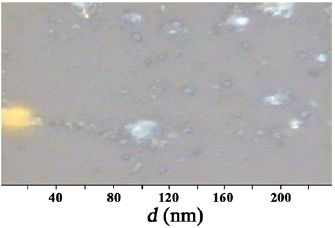
Figure 7. The surface structure of the film, synthesized on a glass substrate from the products of copper electrodes sputtered in atmospheric pressure air during 30 min under the action of nanosecond discharge factors ( ).
).
Download figure:
Standard image High-resolution image
Figure 8. The Raman scattering spectra of nanostructured zinc oxide synthesized on a glass substrate from products of atomization of zinc electrodes in the air during the time 30 min (1) and the Raman scattering spectra of  -based nanostructures on the alund (
 ) substrate, which are given in [24].
Download figure:
Standard image High-resolution imageOur hypothesis has been confirmed for nanostructures based on  after investigating the Raman spectrum of ion argon laser radiation at a wavelength of 514.5 nm and comparing it with the corresponding Raman scattering spectrum of the same laser radiation by nanostructures from
  . In [24], zinc oxide nanostructures were synthesized by the action of a powerful, thinner laser on KrF molecules with a generation wavelength of 248 nm on a continuously rotating
  ceramic target surface.
As follows from figure 8, the obtained by us Raman spectrum of  laser radiation is in good agreement with the data of work [24], where scattering of zinc oxide nanowires with a diameter of 8–35 nm was investigated. The differences in our Raman scattering spectra and the data [24] in the range of wavelengths of
  are due to the different types of substrates on which these nanostructures were synthesized. Therefore, with a large probability, we can assume that in our conditions the synthesis of nanoparticles from ZnO was carried out directly on the glass substrate without the use of transitional film structures with the nuclei for the growth of nanoscale columns.
The transmission spectra of films based on zinc, copper and iron nanostructures in the visible wavelength region are shown in figure 9 [25]. The transmission of the films was studied in the middle of the radius of the substrate. It was found that films radially are rather inhomogeneous, which is due mainly to gas-dynamic phenomena within the discharge gap and the use of a point source of vapor from the material of the electrodes [26]. It is possible to improve the homogeneity of deposited nanostructures radially when the substrate is moved relative to the discharge gap with a certain low velocity and using a ruler of discharge gaps when large-area films are deposited.
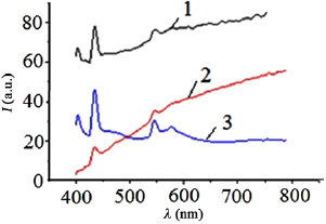
Figure 9. The transmission spectra of films obtained by sputtering copper-1, iron-2 and zinc-3 electrodes in atmospheric pressure air.
Download figure:
Standard image High-resolution imageThe general form of nanostructures bandwidth when film bandwidth sharply increases in the visible range (continuum without maximums and minimums from 500 to 650 nm) corresponds well to cuprous oxide nanostructures bandwidth  [27]. The absorption band of the film in the wavelength range 550–580 nm corresponds to the absorption band of copper nanostructures [28]. Narrow bands of thin film enlightenment in blue part of the spectrum (at wavelengths 420 and 450 nm, most probably due to the action of a plasma discharge ultraviolet radiation in the spectral range 200–230 nm on the film, which during film deposition leads to radiation-induced defects of nanostructured film on the bases of copper oxide and cuprous oxide and the formation of new energy states of these compounds. Nanostructures of copper oxide and cuprous oxide and their colloidal solutions are characterized by broad structureless transmission spectra in the UV, visible and near infrared spectral ranges [29, 30], but not the narrow regions of enlightenment, which were observed in this experiment. The most intense enlightenment bands were nanostructured films based on products of sputtering electrodes from copper and zinc, correlated with selective and intense radiation of a nanosecond discharge in the spectral range 200–230 nm. For the discharge between electrodes made of stainless steel, the selectivity and intensity of the plasma radiation decrease, which leads to a decrease in the film enlightenment maxima on the basis of iron nanostructures (figure 9).
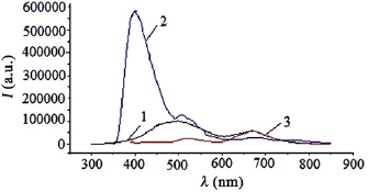
Photoluminescence of nanostructured films based on products of sputtered copper electrodes in air (figure 10) was most efficiently excited from radiation with a wavelength 330 nm.
Figure 10. Photoluminescence spectra of nanostructures based on copper, when excited by radiation with wavelengths 270 (1), 330 (2) and 380 (3) nm.
Download figure:
Standard image High-resolution image
The photoluminescence spectra were characterized by two broad maxima in the spectral range 400–600 nm, which moved to the long-wavelength region of the spectrum and decreased in intensity at transition from the wavelength of the exciting radiation at 330 nm both in the 270 nm region and in the 380 nm region [31]. It was pointed out in [12] that the assisting of the growth of transparent conducting layers on the basis of zinc oxide nanostructures with ultraviolet radiation from a mercury lamp contributes to the improvement of their electrical characteristics through the creation of additional donor centers and a decrease in the scattering of charge carriers at intergranular boundaries of nanowhiskers. In our case, there is no need to use an external source of ultraviolet radiation, since the plasma itself is a selective radiator in the spectral range 200–230 nm.
5. Conclusion
Thus, it has been established that an overstressed nanosecond discharge in air between electrodes from zinc and copper is a selective source of UV radiation in the spectral ranges 200–215 nm and 200–230 nm, respectively; discharge radiation between electrodes of stainless steel filled a relatively wide spectral range 200–300 nm; the maximum pulsed energy input in the plasma is 4 MW, and the energy input in the discharge in one pulse reached 0.1 J; estimates of the plasma parameters on the basis of a numerical solution of the Boltzmann equation for EEDF showed that for the range of the reduced electric field strength (615–820) Td at which the experiments were performed, mean electron energy varies in the range 12.5–16.0 eV, and the electron concentration is in the range  ; the rate constants of the excitation of the energy states of the copper atom and their direct ionization by electron impact are in the range
  ; at
; at  the maximum excitation rate constant for the nitrogen molecule was for the sum of singlet-singlet states
  ; the specific losses of the discharge power for inelastic processes of electron collisions with the components of the mixture were maximal for the nitrogen molecule (32.7%) to excite the sum of the singlet states of the nitrogen molecule; thin films based on nanostructures of copper, zinc and copper and zinc oxides with dimensions 2–40 nm were synthesized; it was found that with the assistance of the deposition of copper films by plasma radiation in the spectral range 200–230 nm, narrow bands of films enlightenment at 420 and 450 nm are formed, which can be due to the formation of radiation defects in these films; the photoluminescence of nanostructured copper films in the visible region of the spectrum was revealed, which was characterized by two maxima at wavelengths in the spectral range 400 and 520 nm, when its excitation occurred with photons with an energy 3.8 eV (at 330 nm); for photons with an energy 2.95 eV a secondary maximum of a smaller amplitude was observed in the luminescence efficiency of films under the action of a high-pressure mercury arc lamp.
Acknowledgments
The authors express their gratitude to Professor Mitsa VM for assistance in studying the characteristics of nanostructures.