

Abstract
This brief overview demonstrates how the ion track-based technology for micro-structuring polymeric materials that has been practised for decades is shifting to the nanometre scale in research and development applications. We present selected results of studies that have focused on the development of new nanoporous materials, especially membranes, performed recently at the Flerov Laboratory of Nuclear Reactions, Joint Institute for Nuclear Research (JINR).
Export citation and abstract BibTeX RIS

Content from this work may be used under the terms of the Creative Commons Attribution-NonCommercial-ShareAlike 3.0 licence. Any further distribution of this work must maintain attribution to the author(s) and the title of the work, journal citation and DOI.
1. Introduction
The present-day field of nanotechnology is an extensive area that comprises a wide spectrum of approaches, utilizing various physical and chemical principles and tools. Accelerated heavy ion beams are one type of tool for modifying materials and they can function on the nanometre scale. There are two opportunities for transforming a material's nanostructure by irradiation with high-energy heavy particles. Firstly, nano-sized alterations can be produced through a direct effect on a crystal lattice due to energy transfer by elastic and inelastic collisions that occur in ion tracks. Secondly, a two-stage treatment can be applied that includes the creation of local radiation damage followed by chemical etching that leads to the formation of the final structure. Etching with heavy ion tracks is a well-known method of producing uniform micro- and nanopores in dielectrics [1, 2]. One of many practical applications of this method is the manufacture of microfiltration membranes (formerly called 'nuclear filters') implemented at the Flerov Laboratory of Nuclear Reactions (FLNR) of JINR in the mid-1970s [3]. Nowadays, the interest of researchers is increasingly focused on the objects characterised by the prefix 'nano-'. This paper is a brief review of the recent achievements by the FLNR in the field of nano- and micro-structured porous materials produced with heavy ion beams.
2. Accelerators
At present, the research activity and the industrial-scale production of track membranes are based on the use of the heavy ion accelerators, U-400 and IC-100, equipped with specialized channels for the irradiation of polymer films. The ion-irradiated films are subject to subsequent physico-chemical treatment (sensitization by ultraviolet radiation and chemical etching). A set of tools (scanning electron microscopy, various porometry methods) is used both for routine control over the quality of irradiation and the parameters of the track membranes (TMs) that are produced, and for the current work aimed at the improvement of the TMs and the development of new nano- and micro-porous materials.
The use of the U-400 for materials modification started in the early 1990s. The cyclotron delivers beams of various ionic species from which krypton and xenon have been selected for routine irradiations (while many others, such as Ca-48, are used in fundamental nuclear physics experiments) [4]. Typically, ion beams with energies of 2.5–5 MeV u −1 are employed. Depending on the specific application, the fluence accumulated in the target varies from about 104 to 1012 cm −2.
In the last decade, a cyclic implanter IC-100 was put into operation at the FLNR. It belongs to a new generation of accelerators and is equipped with a superconducting ECR ion source and a system of external axial injections for the beam. This compact cyclotron with a 1 m pole diameter provides high-intensity beams of multiply charged ions of xenon, krypton, and argon [5] with energies of 1.2 MeV u −1. The intensity of the extracted beams is near 3 μA. A system of beams scanning in two planes has been installed in the transport line of the extracted beam. It provides a homogeneous implantation of ions on a large area of the target (figure 1). Currently, the irradiation of polymeric materials is carried out by Kr 15+ and Xe 23+ ions that have a range of about 16 and 20 μm, respectively, in a polymer (e.g. polyethylene terephthalate). Therefore, the bulk modification of foils 10–20 μm thick and the surface modification of thicker materials can be performed on the IC-100. Accordingly, the ion beams of higher energies from the U-400 are used in cases where a deeper penetration depth is needed.
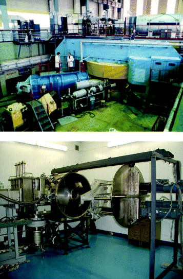
Figure 1 Top: the U-400 cyclotron. Bottom: the set-up for irradiating polymeric foils on the IC-100 accelerator: the vacuum chamber and web transport mechanism [5].
3. Track membranes
The opportunities provided by the two accelerators mentioned above allow for the production of track membranes with a pore density in the range from 104 up to 3×109 cm 2 and a pore diameter from 20 nm up to 5–7 μm (see examples in figure 2). A polyethylene terephthalate film (PET) serves as a raw material for the mass production of track membranes. However, for some special purposes, other materials can be used successfully [6]. For example, polyimide and polyethylene naphthalate track membranes were developed for diffraction filters used in x-ray astronomy [7]. A technology of manufacturing fluoropolymer TMs [8, 9] has also been developed.
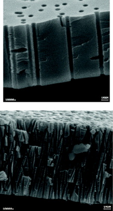
Figure 2 Cross-section of a PET TM with cylindrical parallel pores with a diameter of 0.8 μm (top) and with tilted (crossed) pores with a diameter of 0.3 μm (bottom). The thickness of the membranes is 10 and 12 μm, respectively. The first membrane was prepared for experiments on the propagation of ultrasonic waves through a porous medium [10]. The second one is a conventional microfiltration TM used, for instance, for purifying drinking water [6].
When studying the porous materials, a comprehensive knowledge of the pore size and shape is of fundamental importance. Scanning electron microscopy (SEM) is routinely used to determine the structural characteristics of track-etched membranes. Detailed information about the membrane structure can be obtained by analysis of the images of both the membrane surfaces and the cross-sections. The latter is normally realized by preparation of fractures of the membranes at cryogenic temperatures. However, even under such conditions, polymer samples fail to represent the primary pore structure because of residual strain. To avoid the residual strain, special preparation techniques are developed for typical TM matrices: polyethylene terephthalate, polycarbonate, and polypropylene [11]. The techniques entail embrittlement of the samples using controllable photo-oxidative, thermo-oxidative or radiation-induced degradation of the polymer matrix and subsequent fracturing. Such an approach has made it possible to obtain reliable information about the pore structure in the membrane bulk. The images presented in figures 2, 4–6 and 9 were obtained in this way.
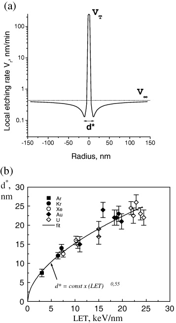
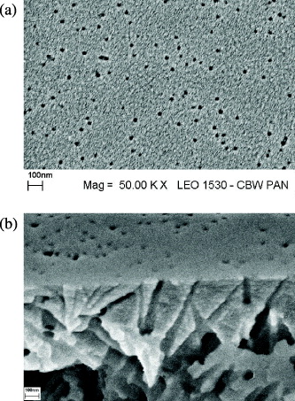
Figure 4 F Structure of a PET membrane with a skin layer obtained using surfactant-controlled etching: surface (a) and cross-sectional view (b). The pore density is 4×109 cm −2. Scale bars: 100 nm [27].
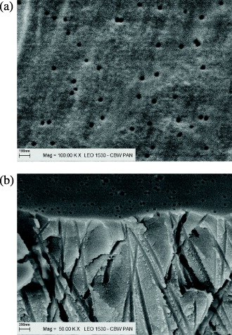
Figure 5 Structure of a PC membrane with a skin layer obtained using surfactant-controlled etching: surface (a) and cross-sectional view (b). The pore density is 2×109 cm −2. Scale bars are 100 nm (a) and 200 nm (b) [27].
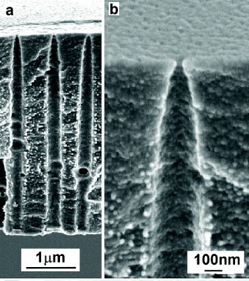
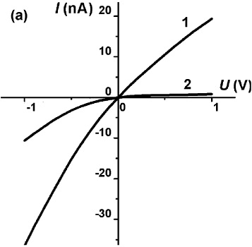
Figure 7 Current–voltage characteristics of asymmetric nanopores with a highly tapered profile in KCl solutions with concentrations of 1 M (1) and 0.1 M (2).
4. The track structure on a nanometre scale
Studies of the macroscopic characteristics of ion-irradiated polymers (PET, polycarbonate, polyolefines, fluoropolymers) have shown that the effects of heavy ions are qualitatively similar in many respects to those caused by radiation with a low linear energy transfer (LET) [12, 13]. This is a natural consequence of the fact that an essential part of the ion energy is transferred to the target through a cascade of secondary electrons that form the so-called track halo. In the ion track halo, the same radiation–chemical reactions take place as under the action of gamma-quanta or electron beams. However, at a high LET, some differences are observed; for example, an essential shift in the balance between the processes of chain rupture and cross-linking towards the latter and a significant growth in the yield of unsaturated bonds in hydrogen-containing polymers. The increase in the probability of cross-linking is probably caused by a high transient concentration of radicals at short distances from the trajectory of the heavy ion, i.e. in the track core. The high yield of unsaturated bonds is a consequence of specific conditions in the core. It is well known that the extremely high density of ionization along the ion path leads to the rapid formation of a narrow (a few nanometres in diameter) positively charged column in which the electrostatic forces initiate a short collision cascade [1]. First of all, a displacement of the lightest atoms and ions, i.e. H and H +, may occur. Therefore, unsaturated structures in the tracks of heavy ions can form by special mechanisms that are distinguished from conventional radiation–chemical reactions. The deep transformation of the polymer's structure in the ion track core results in its ability to selectively chemically etch. Even in such a typical cross-linking polymer as polyethylene, the heavy ions produce tracks that can be selectively developed by chromic acid [13] (though, normally, cross-linking leads to a decrease in solubility and an increase in chemical resistance). This proves that the track core is likely formed due to the physical mechanisms mentioned above. An important property of the track core is an increased free volume [12, 14]. The free volume provides a facilitated transport of the etchant along the axis of the track and an increase in the etch rate in a narrow channel around the ion trajectory. One should note a duality of the properties of the track core: its transverse size is determined by a fast physical process [15, 16] and is practically independent of the secondary reactions following it, while the chemical activity of the substance in the track core essentially depends on the secondary reactions of radiolysis products. This manifests itself by the dependence of the track etch rate on the oxidation in air [1, 6], on the presence of an antioxidant in the polymer [13], and on the temperature during irradiation [17].
The chemical etching method, initially suggested only for the visualization of tracks, has turned out to be quite useful for revealing the spatial structure of heavy ion tracks in the nanometre range. The chemical etching combined with electrical conductance measurements have been applied to investigate the structure of tracks of multi-charged ions with atomic numbers from 18 up to 92 [15, 16, 18–20].
An example of the dependence of the local etch rate, V r , on the distance from the track axis is shown in figure 3(a). Within a zone of a radius of several nanometres, the local rate of dissolution of the damaged material exceeds the etching rate of the pristine polymer by many times. The quantity V r quickly decreases as the radius passes a minimum and then slowly increases, asymptotically approaching a constant value V. The diameter d * of the channel formed at the moment when the local etch rate takes a minimal value is a parameter that is convenient for using as the characteristic size of the central part of the track. This size likely corresponds to the maximal density of cross-linking. The core of the track is surrounded by a diffuse shell (also called a 'halo') in which cross-linking prevails over chain rupture. The radius of the halo is at least an order of magnitude greater than the radius of the selectively etched track core. A dependence of d * on the LET is shown in figure 3(b). On a PET sample, it has been found that the radii of the core and the halo increase approximately proportionally to the square root of the LET as it varies from 3 up to 25 keV nm −1 [15, 18]. For nanotechnological applications, the track core diameter is the most important quantity because it defines a minimal scale of the objects that can be created by etching ion tracks.
For the fabrication of nanoporous bodies with a high aspect ratio, another key parameter is the cone half-angle, [1, 2] which, in turn, depends on the track etch ratio. The latter is defined as the ratio of the track etch rate V T and the bulk etch rate V. The bulk etch rate depends on the material, on the etchant composition and on the temperature. The track etch rate depends on a much greater number of factors, which include sensitivity of the material, irradiation conditions, post-irradiation conditions, and etching conditions. High LET of the bombarding particle is the most important prerequisite to achieve a high aspect ratio. The track etch rate increases with increasing LET. However, at very high LET values (∼10 keV nm −1), this quantity tends to saturation or may even show a maximum in some materials [6]. Aromatic polymers having relatively weak ester bonds in the backbone chain—polyethylene terephthalate, polycarbonate, polyethylene naphthalate—show the track etch ratio as high as thousands under optimal processing conditions. Another group of polymers, such as polyimide, polypropylene and polyvinylidene fluoride, hold an intermediate position with regard to the track etching selectivity: typically, track etch ratio values of hundreds can be achieved. Lastly, there is a group of technologically important polymers in which even high-LET ions do not produce highly etchable tracks. These are chemically and thermally resistant plastics (polysulfone, polyphenylene oxide, polyetherether ketone) to which the track etching technique has not yet been successfully applied [21].
5. New types of membranes with pores smaller than 100 nm
In the last few years, procedures have been developed that allow one to produce 'track' nanopores with a controllable longitudinal profile in polymeric films [22–28]. It has been shown that adding surfactants to etching solutions makes it possible to essentially change the process of pore growth. Aggregates of surfactant molecules formed at the track entrance represent a barrier to penetration into the track of relatively large molecules, while the hydroxide ions diffuse freely into the growing nanopore. The profile of the formed nanochannels depends on the alkali concentration, the temperature, and the type of surfactant. By varying the conditions, one can control the shape of the channel. The developed method allows one to optimize the pore shape in track membranes and to improve their operational characteristics. Excluding surfactant sorption on one membrane side, one can fabricate asymmetrical high-performance track membranes with a thin selective layer(figures 4 and 5). The thickness of the selective layer is about 1 μm, while the channel diameter can change, for example, from 20 nm on a selective surface up to 80–100 nm in the membrane bulk. An optimal ratio of the pore diameter in the selective layer to the diameter in the bulk is found from a condition of maximal flow rate at a fixed volume porosity of TM [25]. Experiments on the ultrafiltration of protein solutions have shown that this new type of track membrane holds a great deal of potential [24].
In order to clarify the question about the surfactant aggregation mechanism and its action on the track pore shapes, small angle neutron scattering experiments were performed. The obtained experimental results allowed clarification of some features of track etching with surfactant-containing solutions. The data on micelle formation under different conditions made it possible to recognize the correlation between the shape of the pores and the peculiarities of the self-assembly of surfactant molecules in the pores, at the surface, and in the bulk solution [28, 29].
To provide improved membrane robustness, allow miniaturization, and allow the possibility of integration with other ionic and electronic devices, silicon-based platforms are the perfect choice. With this in mind, attempts have been made to develop nanopore TMs of silicon nitride. Because of the extremely high radiation resistance of SiN, we succeeded in getting a satisfactory nanopore structure by irradiating silicon nitride films with particles as heavy as bismuth ions at an energy of 710 MeV (LET≈ 36 keV nm −1) [30]. The obtained ultrathin freestanding SiN membranes (thickness of 200–300 nm, pore diameter of 3–20 nm) feature excellent selectivity in filtration processes based on the permeation charge and size. Negatively charged membranes distinguish between the positively charged Rhodamine dye and the negative Alexa fluorophor, so that only the positive molecule is transported. The membranes also act as molecular sieves by selecting the smaller BSA over the larger IgG protein [30].
Although they have been studied for decades, narrow pores with charged walls exhibit surprising properties that are not yet fully understood. A study of the passive diffusion of low-molecular-weight organic compounds through a PET track-etched membrane with a pore size of 30 nm has shown that the transport of the compounds is realized through their accumulation in the membrane pores [31]. Aniline molecules, which are neutral in the bulk solution, diffuse through the membrane in cationic form. The accumulation of penetrants in nanopores may give rise to new applications of track-etched membranes. Membrane nanoreactors may be based on the preconcentration of initially diluted reactants in the course of their diffusive transport with a subsequent chemical reaction in the pores. Upon preconcentration, the reactants may undergo the desired transformations [31]. The possible applications of such a membrane could vary from technology to analytical chemistry.
6. The asymmetric nanopore as a 'nanofluidic device'
Attempts to model ion channels in biological membranes using artificial pores in synthetic materials have resulted in quite interesting discoveries about the properties of asymmetric track-etched nanopores [32–35]. Filled with a solution of electrolyte, the conical pores with tips of several nanometres in diameter demonstrate a pronounced effect of rectification of the electrical current [33–35]. This property is related to the presence of dissociating carboxyl groups on the pore walls, which cause a negative surface charge. For ion current rectification to occur, one lateral dimension of the pore is on the nanoscale, and a geometric or surface charge asymmetry exists along the ion current flow direction. The asymmetrical track-etched pores are considered good candidates for mimicking the transport of ions and neutral molecules in biological ion channels and for the development of bioinspired intelligent nanomachines, such as biosensors and nanofluidic devices. The ion track technique provides a simple and reliable fabrication method for profiled (asymmetrical) pores, and the pore size, taper angle, and channel geometry can be controlled by recently developed etching methods. As opposed to the traditional objects that biophysicists still use to study properties of biological membranes, polymer films with track-etched pores are more 'robust', mechanically rigid, and chemically resistant, and thus they are better suited to repeated measurements under various conditions.
We have developed a technique for fabricating asymmetric track-etched nanopores with a highly tapered profile (see figure 6), which may be promising for sensing and nanofluidic applications [36, 37]. The rectification ratio exhibited by the highly tapered nanopores is higher than that of conical pores, which suggests that the pores with a bullet-like geometry are better nanofluidic diodes than the conical pores developed before. Further measurements of the pores with controlled shapes may help to better relate the theoretical models to the experimental data [38]. The novel process offers new possibilities for controlling the pore geometry. In the case of a convex profile, like that shown in figure 6, the effective length of the narrow tip of the pore can be made small, which is important when the pore is used as a sensing element.
7. Asymmetric nanopores in molecular sensors and projection nanolithography
This type of nanostructure has attracted the increasing interest of researchers due to the problem of detection and identification of biologically important molecules. If the radius of the channel is compatible with the molecule size, the molecule can be registered at the moment of passing the pore in a way that is similar to that by which molecules are counted in a Coulter counter with a suspension of colloidal particles. For long chain molecules, for instance DNA, the opportunity of reading a sequence of nucleotides by such a method is currently under discussion. The implementation of this idea would allow a revolutionary simplification of the DNA analysis technique and reduce its cost [39].
Apart from resistive-pulse sensing, the shaped nanopores can find other applications where small uniform apertures in a thin partition are needed. An example of such an application is an atom 'pinhole camera (or 'obscure camera') with nanometre resolution that has been experimentally implemented based on an asymmetric track-etched membrane [40, 41]. In the atom 'pinhole camera', an atomic beam is transmitted through a shaped hole ('object') in a metal mask, thus forming, by analogy with optics, a 'luminous object' of a specified geometry. The atoms transmitted through the hole in the mask propagate in a vacuum over straight-line trajectories and arrive at a thin film located at a distance L from the mask with a large number of nano-apertures. Each nano-aperture in the film serves as an obscure camera for atoms, forming an individual image of the 'object' on the surface of a substrate, which is located at a small distance l behind the film. In this geometry, a set of object images, reduced approximately by a factor of m=L / l, is formed on the substrate. We used a thin film with nano-apertures as an asymmetrical track membrane with a thickness of 5 μm and a tip diameter d=50 nm. Figure 8 gives an example of an image obtained with a reduction factor of 8000. It should be noted that the number of pores in the TM can be very large (∼108 cm −2) and, therefore, the parallel nanofabrication of an array of identical objects can be performed.
Figure 8 Nanostructures in the form of the Greek letter λ composed of Cr atoms. The figure was obtained with an asymmetric nanopore track-etched membrane used as an obscure camera [40]. Substrate: glass surface.
For the parallel nanofabrication methods, an array of nano-apertures with a regular spatial distribution is favoured, whereas the normal ion irradiation technique distributes ion tracks at random [42]. The microbeam facility built at the GSI Helmholtz Zentrum fuer Schwerionenforschung (Darmstadt, Germany) allows a 'deterministic' irradiation so that a regular pattern of a pre-set number of single tracks placed at certain distances is produced [43, 44]. SEM images in figure 9 show the appearance of the membranes having highly asymmetric conical pores spaced at 5 μm intervals. Due to the conical shape, the narrow pore tips are quite short and can be considered as pinholes in thin partition to be used in the atomic beam optics.
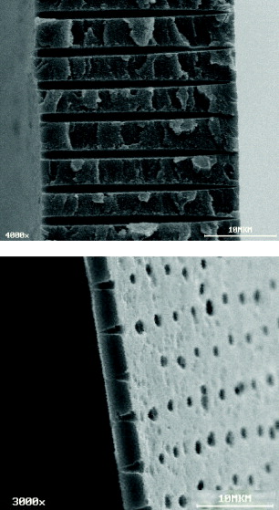
Figure 9 Arrays of regularly distributed conical pores produced using microbeam irradiation [43, 44] and asymmetrical etching [37]. Top: polycarbonate foil 28 μm thick. Bottom: PET foil 4 μm thick. The larger pore diameter is about 2 μm, and the smaller pore diameter is about 50 nm in both membranes. The smaller pore diameter is below the observation limit at the magnification used. Scale bars: 10 μm.
8. Conclusion
The ion track-based technology for micro-structuring polymeric materials that has been practised for decades is developing into the research and development of nanoscale materials. Because the characteristic radius of the ion track is several nm, energetic heavy ions are a powerful 'nanotool' for transforming the structure and properties of materials. In the past few years, some promising research areas have appeared in which the use of heavy ion beams can generate interesting practical results. One can expect that the progress of these studies and the search for new applications will make a noticeable contribution to the development of nanotechnology.
Acknowledgments
We express our gratitude for fruitful cooperation in the field of ion track nanotechnological applications to our partners: the Materials Research Group (das GSI Helmholtz Zentrum fuer Schwerionenforschung, Darmstadt), the Department of Membrane Technologies of the AV Shubnikov Institute of Crystallography RAS (Moscow), the Laboratory of Laser Spectroscopy of the Institute of Spectroscopy RAS (Troitsk), the Institute of Nuclear Chemistry and Technology (Warsaw), the Department of Physics and Astronomy, University of California (Irvine), and the M V Lomonosov Moscow State University. The work was performed under the partial support of the Russian Foundation for Basic Research (grants nos 05-08-18030-a, 06-08-01299-a, 06-08-07094-3, and 07-03-00743-a).